Nexperia
PRTR5V0U2X-Q
Ultra low capacitance double rail-to-rail ESD protection diode
10. Application information
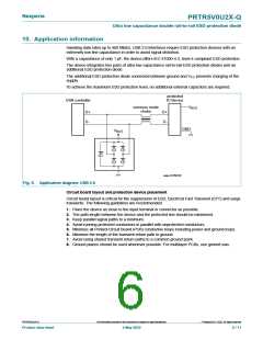
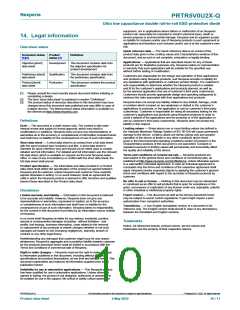
Handling data rates up to 480 Mbit/s, USB 2.0 interfaces require ESD protection devices with an
extremely low line capacitance in order to avoid signal distortion.
With a capacitance of only 1 pF, the device offers IEC 61000-4-2, level 4 compliant ESD protection.
The device integrates two pairs of ultra low capacitance rail-to-rail ESD protection diodes and an
additional ESD protection diode.
The additional ESD protection diode connected between ground and VCC prevents charging of the
supply.
To achieve the maximum ESD protection level, no additional external capacitors are required.
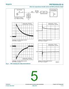
protected
USB controller
IC/device
common mode
choke
V
BUS
D+
D-
D+
D-
GND
V
BUS
aaa-035030
Fig. 5. Application diagram: USB 2.0
Circuit board layout and protection device placement
Circuit board layout is critical for the suppression of ESD, Electrical Fast Transient (EFT) and surge
transients. The following guidelines are recommended:
1. Place the device as close to the input terminal or connector as possible.
2. The path length between the device and the protected line should be minimized.
3. Keep parallel signal paths to a minimum.
4. Avoid running protected conductors in parallel with unprotected conductors.
5. Minimize all Printed-Circuit Board (PCB) conductive loops including power and ground loops.
6. Minimize the length of the transient return path to ground.
7. Avoid using shared transient return paths to a common ground point.
8. Ground planes should be used whenever possible. For multilayer PCBs, use ground vias.
©
PRTR5V0U2X-Q
All information provided in this document is subject to legal disclaimers.
Nexperia B.V. 2022. All rights reserved
Product data sheet
4 May 2022
6 / 11

 NEXPERIA [ Nexperia ]