Nexperia
PRTR5V0U2X-Q
Ultra low capacitance double rail-to-rail ESD protection diode
9. Characteristics
Table 6. Characteristics
Symbol
VF
Parameter
Conditions
Min
Typ
0.7
-
Max
-
Unit
V
forward voltage
breakdown voltage
reverse current
Tamb = 25 °C
-
VBR
[1]
[2]
6
-
9
V
IR
VR = 3 V; Tamb = 25 °C
< 1
1
100
1.5
nA
pF
C(I/O-GND)
input/output to ground f = 1 MHz; V(I/O-GND) = 0 V; Tamb = 25 °C [3]
capacitance
-
C(I/O-I/O)
Csup
input/output to input/
output capacitance
f = 1 MHz; V(I/O-I/O) = 0 V; Tamb = 25 °C [4]
-
-
0.6
16
-
-
pF
pF
supply pin to ground
capacitance
f = 1 MHz; Vcc = 0 V; Tamb = 25 °C
[1]
VCL
clamping voltage
IPPM = 2.5 A; 8/20 µs; Tamb = 25 °C
IPPM = -2.2 A; 8/20 µs; Tamb = 25 °C
[5]
[5]
-
-
17
-4
-
-
V
V
[1] Measured from pin 4 to ground.
[2] Measured from pin 2, 3 and 4 to ground.
[3] Measured from pin 2 and 3 to ground.
[4] Measured from pin 2 to pin 3.
[5] Device stressed with 8/20 μs exponential decay waveform according to IEC 61000-4-5.
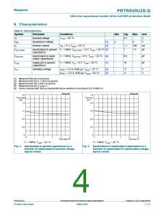
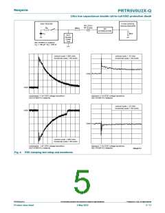
006aaa483
006aaa484
2.0
1.0
C
C
(I/O-GND)
(pF)
(I/O-I/O)
(pF)
1.6
1.2
0.8
0.4
0
0.8
0.6
0.4
0.2
0
0
1
2
3
4
5
(V)
0
1
2
3
4
5
(V)
V
V
(I/O-I/O)
(I/O-GND)
f = 1 MHz; Tamb = 25 °C
f = 1 MHz; Tamb = 25 °C
Fig. 2. Input/output to ground capacitance as a
function of input/output to ground voltage;
typical values
Fig. 3. Input/output to input/output capacitance as a
function of input/output to input/output voltage;
typical values
©
PRTR5V0U2X-Q
All information provided in this document is subject to legal disclaimers.
Nexperia B.V. 2022. All rights reserved
Product data sheet
4 May 2022
4 / 11

 NEXPERIA [ Nexperia ]