Nexperia
BAS316
High-speed switching diode
mbg446
006aab133
2
10
0.8
I
R
(1)
(2)
C
(pF
d
(µA)
10
)
0.6
0.4
1
-1
10
10
10
10
10
(3)
(4)
-2
-3
-4
-5
0.2
0
0
4
8
12
16
0
20
40
60
80
100
V
R
(V)
V
(V)
R
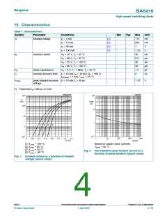
(1) Tamb = 150 °C
(2) Tamb = 85 °C
(3) Tamb = 25 °C
(4) Tamb = -40 °C
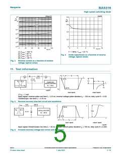
f = 1 MHz; Tamb = 25 °C
Fig. 4. Diode capacitance as a function of reverse
voltage; typical values
Fig. 3. Reverse current as a function of reverse
voltage; typical values
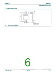
11. Test information
t
r
t
p
t
D.U.T.
10 %
I
+ I
F
t
F
rr
R
S
= 50 Ω
SAMPLING
OSCILLOSCOPE
t
R
i
= 50 Ω
V = V + I × R
S
R
F
(1)
90 %
V
R
mga881
input signal
output signal
(1) IR = 1 mA
Input signal: reverse pulse rise time tr = 0.6 ns; reverse voltage pulse duration tp = 100 ns; duty cycle δ = 0.05
Oscilloscope: rise time tr = 0.35 ns
Fig. 5. Reverse recovery time test circuit and waveforms
I
1 kΩ
450 Ω
I
V
90 %
R
S
= 50 Ω
OSCILLOSCOPE
= 50 Ω
V
FR
D.U.T.
R
i
10 %
t
t
t
t
p
r
input signal
output signal
mga882
Input signal: forward pulse rise time tr = 20 ns; forward current pulse duration tp ≥ 100 ns; duty cycle δ ≤ 0.005
Fig. 6. Forward recovery voltage test circuit and waveforms
©
BAS316
All information provided in this document is subject to legal disclaimers.
Nexperia B.V. 2022. All rights reserved
Product data sheet
1 July 2022
5 / 10

 NEXPERIA [ Nexperia ]