Nexperia
74AHC08-Q100; 74AHCT08-Q100
Quad 2-input AND gate
Table 7.
Dynamic characteristics …continued
GND = 0 V; For test circuit see Figure 7.
Symbol Parameter Conditions
25 C
40 C to +85 C 40 C to +125 C Unit
Min Typ[1] Max Min
Max
Min
Max
For type 74AHCT08-Q100
[2]
[3]
tpd
propagation nA, nB to nY; see Figure 6
delay
VCC = 4.5 V to 5.5 V
CL = 15 pF
-
-
-
3.2
4.2
6.9
7.9
-
1.0
1.0
-
8.0
9.0
-
1.0
1.0
-
9.0
10.0
-
ns
ns
pF
CL = 50 pF
CPD
power
dissipation
capacitance
CL = 50 pF; fi = 1 MHz;
VI = GND to VCC
12.0
[1] Typical values are measured at nominal supply voltage (VCC = 3.3 V and VCC = 5.0 V).
[2] tpd is the same as tPLH and tPHL
.
[3] CPD is used to determine the dynamic power dissipation (PD in W).
PD = CPD VCC2 fi N + (CL VCC2 fo) where:
fi = input frequency in MHz, fo = output frequency in MHz
CL = output load capacitance in pF
VCC = supply voltage in Volts
N = number of inputs switching
(CL VCC2 fo) = sum of the outputs.
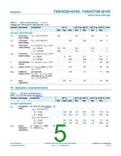
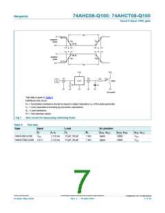
11. Waveforms
V
I
V
nA, nB input
GND
M
t
t
PLH
PHL
V
OH
nY output
V
M
V
OL
mna224
Measurement points are given in Table 8.
OL and VOH are typical voltage output levels that occur with the output load.
V
Fig 6. The input (nA, nB) to output (nY) propagation delays
Table 8.
Type
Measurement points
Input
VM
Output
VM
74AHC08-Q100
74AHCT08-Q100
0.5VCC
1.5 V
0.5VCC
0.5VCC
74AHC_AHCT08_Q100
All information provided in this document is subject to legal disclaimers.
©
Nexperia B.V. 2017. All rights reserved
Product data sheet
Rev. 1 — 16 April 2013
6 of 14

 NEXPERIA [ Nexperia ]