Nexperia
74AHC08-Q100; 74AHCT08-Q100
Quad 2-input AND gate
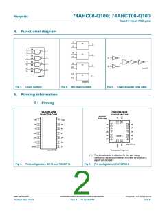
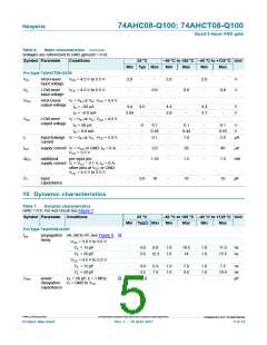
4. Functional diagram
1
&
&
&
&
3
6
2
1
2
1A
1B
1Y
2Y
3Y
3
6
8
4
5
4
5
2A
2B
A
B
Y
9
3A
3B
9
10
8
10
mna221
12
13
4A
4B
4Y 11
12
13
11
mna222
mna223
Fig 1. Logic symbol
Fig 2. IEC logic symbol
Fig 3. Logic diagram (one gate)
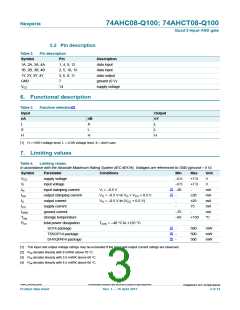
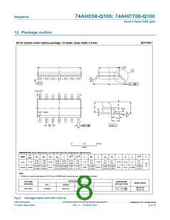
5. Pinning information
5.1 Pinning
ꢀꢁꢂꢃꢄꢅꢆꢇꢈꢉꢅꢅ
ꢀꢁꢂꢃꢄꢊꢅꢆꢇꢈꢉꢅꢅ
ꢀꢁꢂꢃꢄꢅꢆꢇꢈꢉꢅꢅ
ꢀꢁꢂꢃꢄꢊꢅꢆꢇꢈꢉꢅꢅ
ꢍꢌꢇ#ꢑꢉꢈ$ꢎꢄ
ꢑꢉ%ꢌ&ꢎꢈꢇꢌꢈ
ꢀ
ꢇ
ꢈ
ꢅ
ꢌ
ꢍ
ꢎ
ꢀꢅ
ꢀꢈ
ꢀꢇ
ꢀꢀ
ꢀꢐ
ꢑ
ꢀꢁ
ꢀꢄ
ꢂ
ꢃꢃ
ꢅꢄ
ꢅꢁ
ꢅꢆ
ꢈꢄ
ꢈꢁ
ꢈꢆ
ꢄꢗ
ꢓ
ꢕ
ꢘ
ꢝ
ꢛ
ꢄꢕ ꢘꢗ
ꢄꢓ ꢘꢖ
ꢄꢔ
ꢓꢖ
ꢓꢗ
ꢓꢔ
ꢀꢆ
ꢄꢄ
ꢘꢔ
ꢄ ꢕꢗ
ꢕꢖ
ꢇꢁ
ꢃꢄꢅ
ꢀꢁꢂ
ꢇꢄ
ꢜ
ꢇꢆ
ꢀꢀꢀꢁꢂꢂꢃꢄꢅꢇ
ꢏ
ꢉꢊꢋ
ꢆꢇꢈꢉꢊꢋꢈꢇꢌꢉꢍꢎꢍꢏꢋꢎꢐꢑꢌꢒ
ꢀꢀꢀꢁꢂꢂꢃꢄꢅꢆ
(1) The die substrate is attached to this pad using
conductive die attach material. It cannot be used as a
supply pin or input.
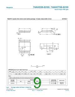
Fig 4. Pin configuration SO14 and TSSOP14
Fig 5. Pin configuration DHVQFN14
74AHC_AHCT08_Q100
All information provided in this document is subject to legal disclaimers.
©
Nexperia B.V. 2017. All rights reserved
Product data sheet
Rev. 1 — 16 April 2013
2 of 14

 NEXPERIA [ Nexperia ]