Nexperia
74AHC08-Q100; 74AHCT08-Q100
Quad 2-input AND gate
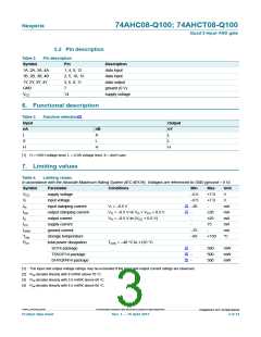
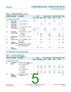
5.2 Pin description
Table 2.
Pin description
Symbol
Pin
Description
1A, 2A, 3A, 4A
1B, 2B, 3B, 4B
1Y, 2Y, 3Y, 4Y
GND
1, 4, 9, 12
2, 5, 10, 13
3, 6, 8, 11
7
data input
data input
data output
ground (0 V)
supply voltage
VCC
14
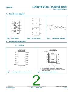
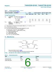
6. Functional description
Table 3.
Function selection[1]
Input
nA
L
Output
nB
X
nY
L
X
L
L
H
H
H
[1] H = HIGH voltage level; L = LOW voltage level; X = don’t care
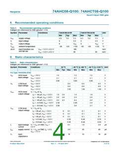
7. Limiting values
Table 4.
Limiting values
In accordance with the Absolute Maximum Rating System (IEC 60134). Voltages are referenced to GND (ground = 0 V).
Symbol
VCC
VI
Parameter
Conditions
Min
0.5
0.5
20
-
Max
+7.0
+7.0
-
Unit
V
supply voltage
input voltage
V
[1]
[1]
IIK
input clamping current
output clamping current
output current
VI < 0.5 V
mA
mA
mA
mA
mA
C
IOK
VO < 0.5 V or VO > VCC + 0.5 V
VO = 0.5 V to (VCC + 0.5 V)
20
25
75
IO
-
ICC
supply current
-
IGND
Tstg
Ptot
ground current
75
65
-
storage temperature
total power dissipation
SO14 package
+150
Tamb = 40 C to +125 C
[2]
[3]
[4]
-
-
-
500
500
500
mW
mW
mW
TSSOP14 package
DHVQFN14 package
[1] The input and output voltage ratings may be exceeded if the input and output current ratings are observed.
[2] Ptot derates linearly with 8 mW/K above 70 C.
[3] Ptot derates linearly with 5.5 mW/K above 60 C.
[4]
Ptot derates linearly with 4.5 mW/K above 60 C.
74AHC_AHCT08_Q100
All information provided in this document is subject to legal disclaimers.
©
Nexperia B.V. 2017. All rights reserved
Product data sheet
Rev. 1 — 16 April 2013
3 of 14

 NEXPERIA [ Nexperia ]