µPD75216A
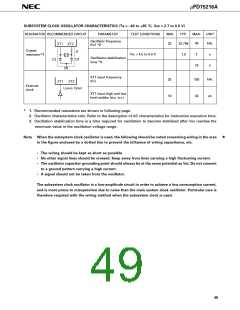
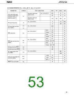
SUBSYSTEM CLOCK OSCILLATOR CHARACTERISTICS (Ta = –40 to +85 °C, VDD = 2.7 to 6.0 V)
MAX.
35
RECOMMENDED CIRCUIT
MIN.
32
TYP.
UNIT
kHz
RESONATOR
PARAMETER
TEST CONDITIONS
Oscillator frequency
(fXT) *2
32.768
XT1
XT2
Crystal
resonator*1
R
VDD = 4.5 to 6.0 V
s
s
2
1.0
Oscillation stabilization
time *3
C3
C4
10
XT1 input frequency
(fXT)
kHz
100
32
32
10
XT1 XT2
Leave Open
External
clock
XT1 input high and low
level widths (tXTH, tXTL)
µs
*
1. Recommended resonators are shown in following page.
2. Oscillator characteristics only. Refer to the description of AC characteristics for instruction execution time.
3. Oscillation stabilization time is a time required for oscillation to become stabilized after VDD reaches the
minimum value in the oscillation voltage range.
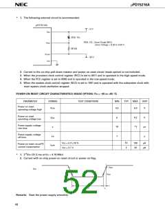
Note When the subsystem clock oscillator is used, the following should be noted concerning wiring in the area
in the figure enclosed by a dotted line to prevent the influence of wiring capacitance, etc.
★
• The wiring should be kept as short as possible.
• No other signal lines should be crossed. Keep away from lines carrying a high fluctuating current.
• The oscillator capacitor grounding point should always be at the same potential as VSS. Do not connect
to a ground pattern carrying a high current.
• A signal should not be taken from the oscillator.
The subsystem clock oscillator is a low-amplitude circuit in order to achieve a low consumption current,
and is more prone to misoperation due to noise than the main system clock oscillator. Particular care is
therefore required with the wiring method when the subsystem clock is used.
49

 NEC [ NEC ]