µPD75216A
*
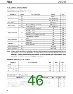
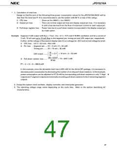
1. Calculation of total loss
Design so that the sum of the following three power consumption values for the µPD75216ACW/GF will be
less than the total loss PT (It is recommended to use the system with 80 % or less of the rating).
➀ CPU loss
: Given as VDD (MAX.) × IDD1 (MAX.)
➁ Output pin loss
: There are normal output pin loss and display output pin loss. It is necessary
to add a loss derived from the flow of maximum current to each output pin.
➂ Pull-down register loss : Power loss due to a pull-down resistor incorporated in the display output pin
by mask option.
Example Suppose 4-LED output with 9SEG × 11DIGIT, VDD = 5 V + 10 % and 4.19 MHz oscillation and let a current of
3 mA, 15 mA and up to 10 mA flow to the segment pin, timing pin and LED output pin, respectively.
Further, let the voltage of fluorescent display tube (VLOAD voltage) be –30 V and normal voltage be small.
➀
➁
CPU loss : 5.5 V × 9.0 mA = 49.5 mW
Pin loss : Segment pin ..... 2V × 3 mA × 9 = 54 mW
Timing pin......... 2V × 15 mA = 30 mW
10
× 2 V × 10 mA × 4 = 53 mW
LED output ........
15
(30 + 5.5V)2
× 10 = 504.1 mW
➂
Pull-down resistor loss ........
25 kΩ
PT = ➀+ ➁ + ➂ = 690.6 mW
In this example, since the allowable total loss is 600 mW for the shrink DIP package, it is necessary to
decrease power consumption by decreasing the number of on-chip pull-down resistors. In this example,
power consumption can be adjusted to 577.8 mW by incorporating pull-down resistors in only 11 digit
outputs and 7 segment outputs and externally mounting pull-down resistors to the 2 remaining segment
outputs.
★
2. Except the system clock oscillator, display controller and timer/pulse generator.
3. The operating voltage range varies depending on the cycle time. Refer to the section describing AC
characteristics.
47

 NEC [ NEC ]