µPD75216A
12. ELECTRICAL SPECIFICATIONS
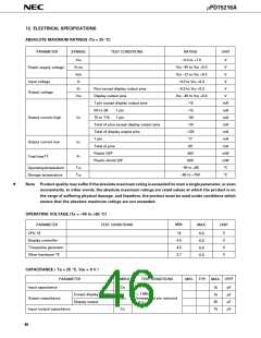
ABSOLUTE MAXIMUM RATINGS (Ta = 25 °C)
PARAMETER
SYMBOL
TEST CONDITIONS
RATING
UNIT
VDD
VLOAD
VPRE
VI
–0.3 to +7.0
V
V
VDD –40 to VDD +0.3
Power supply voltage
VDD –12 to VDD +0.3
V
Input voltage
–0.3 to VDD +0.3
V
VO
Pins except display output pins
Display output pins
–0.3 to VDD +0.3
V
Output voltage
VOD
VDD –40 to VDD +0.3
V
1 pin except display output pins
–15
–15
mA
mA
mA
mA
mA
mA
mA
mW
mW
°C
S0 to S9
1 pin
1 pin
IOH
T0 to T15
–30
Output current high
Total of pins except display output pins
Total of display output pins
1 pin
–20
–120
17
Output current low
IOL
PT
Total of pins
60
Plastic QFP
450
Total loss*1
Plastic shrink DIP
600
Topt
Tstg
–40 to +85
–65 to +150
Operatingtemperature
Storage temperature
°C
Note Product quality may suffer if the absolute maximum rating is exceeded for even a single parameter, or even
momentarily. In other words, the absolute maximum ratings are rated values at which the product is on
the verge of suffering physical damage, and therefore, the product must be used under conditions which
ensure that the absolute maximum ratings are not exceeded.
★
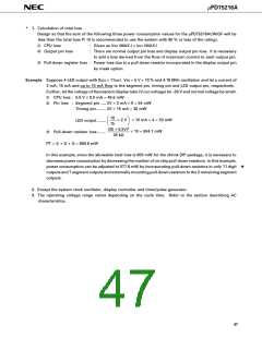
OPERATING VOLTAGE (Ta = –40 to +85 °C)
MIN.
PARAMETER
CPU *2
MAX.
TEST CONDITIONS
UNIT
V
V
V
V
*3
4.5
4.5
2.7
6.0
6.0
6.0
6.0
Display controller
Time/pulse generator
Other hardware *2
CAPACITANCE ( Ta = 25 °C, VDD = 0 V )
UNIT
MAX.
PARAMETER
SYMBOL
TEST CONDITIONS
MIN.
TYP.
Input capacitance
CIN
pF
pF
pF
pF
15
15
35
15
f = 1 MHz
Unmeasured pin returned
to 0 V
Except display output
Output capacitance
Display output
COUT
CIO
Input /output capacitance
46

 NEC [ NEC ]