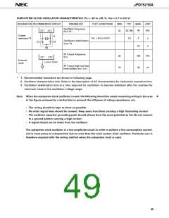
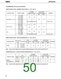
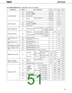
µPD75216A
*
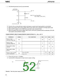
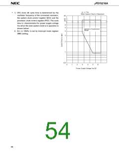
1. The following external circuit is recommended.
µPD75216A
+5 V
VDD
RD9, 1EL
RD9, 1EL : Zener Diode (NEC)
V
PRE
Zener Voltage = 8.29 to 9.30 V
68 kΩ
VLOAD
–30 V
V
SS
2. Current to the on-chip pull-down resistor and power-on reset circuit (mask option) is not included.
3. When the processor clock control register (PCC) is set to 0011 and is operated in the high-speed mode.
4. When the PCC register is set to 0000 and is operated in the low-speed mode.
5. When the system clock control register (SCC) is set to 1001 and is operated with the subsystem clock with
main system clock oscillation stopped.
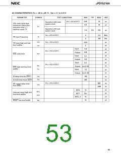
POWER-ON RESET CIRCUIT CHARACTERISTICS (MASK OPTION) (Ta = –40 to +85 °C)
PARAMETER
SYMBOL
TEST CONDITIONS
MIN.
4.5
TYP.
MAX.
6.0
UNIT
V
Power-on reset
operating voltage high
VDDH
Power-on reset
operating voltage low
0.2
V
0
10
1
VDDL
tr
Power supply voltage
rise time
*1
µs
Power supply voltage
off time
toff
s
10
2
VDD = 5 V ±10 %
100
20
µA
µA
Power-on reset circuit*2
current consumption
IDDPR
VDD = 2.7 V
*
1. 217/fXX (31.3 ms at fXX = 4.19 MHz)
2. Current with on-chip power-on reset circuit or power-on flag.
V
DDH
V
DD
V
DDL
t
off
t
r
Remarks Start the power supply smoothly.
52

 NEC [ NEC ]