µPD75216A
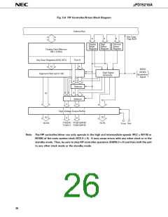
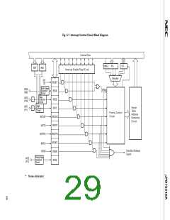
Fig. 5-8 FIP Controller/Driver Block Diagram
Internal Bus
Key Scan
Flag (KSF)
4
4
4
Display
Mode
Register
Digit
Dimmer
Select
Register
Select
Register
Display Data Memory
(64 × 4 Bits)
Key Scan Registers (KS0, KS1)
12
Port H
4
INTKS
IRQKS
Generation
Signal
Digit Signal
Generator
Segment Data Latch (16)
4
4
Selector
2
2
4
4
10
Selector
4
10
2
High-Voltage Output Buffer
10
10
2
4
T15/S10, T13/S12/PH0-
T14/S11 T10/S15/PH3
T0-T9
S0-S9
V
LOAD
V
PRE
Note The FIP controller/driver can only operate in the high and intermediate-speeds (PCC = 0011B or
0010B) of the main system clock (SCC.0 = 0). It may cause errors with any other clock or in the
standby mode. Thus, be sure to stop FIP controller operation (DSPM.3 = 0) and then shift the unit
to any other clock mode or the standby mode.
26

 NEC [ NEC ]