µPD75216A
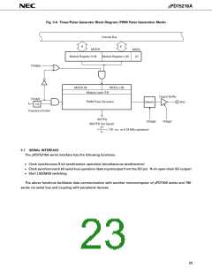
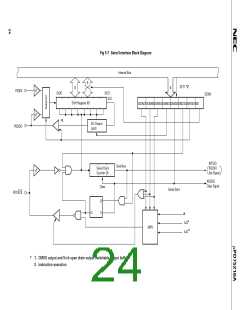
Fig. 5-6 Timer/Pulse Generator Block Diagram (PWM Pulse Generation Mode)
Internal Bus
8
8
MODH
MODL
(2)
Modulo Register H (8)
Modulo Register L (6)
TPGM3
MODH (8)
Modulo Latch (14)
MODL7-2 (6)
Output Buffer
TPGM1
1/2
PWM Pulse Generator
Selector
TPGM5
PPO
fx
Frequency Divider
INTTPG
(IRQTPG Set Signal)
215
TPGM7
(
= 7.81 ms : at 4.19 MHz operation)
f
X
5.7 SERIAL INTERFACE
The µPD75216A serial interface has the following functions.
•
•
•
Clock synchronous 8-bit send/receive operation (simultaneous send/receive)
Clock synchronous 8-bit serial bus operation (data input/output from the SO pin. N-ch open-drain SO output)
Start LSB/MSB switching
The above functions facilitates data communication with another microcomputer of µPD7500 series and 78K
series via serial bus and coupling with peripheral devices.
23

 NEC [ NEC ]