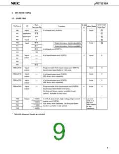
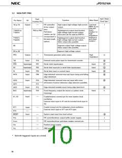
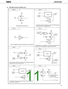
µPD75216A
3.5 P00/INT4 PIN AND RESET PIN OPERATING PRECAUTIONS
P00/INT4 and RESET pins have the function (especially for IC test) to test µPD75216A internal operations in
addition to the functions described in sections 3.1 and 3.2.
The test mode is set when a voltage larger than VDD is applied to one of these pins. If noise larger than VDD is
applied in normal operation, the test mode may be set thereby adversely affecting normal operation.
Since there is a display output pin having a high-voltage amplitude (35 V) next to the P00/INT4 and RESET pins,
if cables for the related signals are routed in parallel, wiring noise larger than VDD may be applied to the P00/INT4
and RESET pins causing errors.
Thus, carry out wiring so that wiring noise can be minimized, If noise still cannot be suppressed, take the measure
against noise using the following external components.
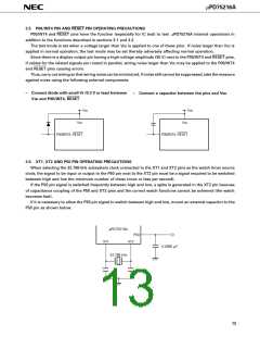
•
Connect diode with small VF (0.3 V or less) between
VDD and P00/INT4, RESET
•
Connect a capacitor between the pins and VDD.
VDD
VDD
VDD
VDD
P00/INT4, RESET
P00/INT4, RESET
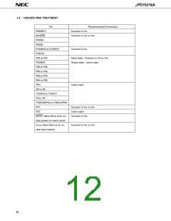
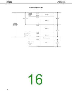
3.6 XT1, XT2 AND P50 PIN OPERATING PRECAUTIONS
When selecting the 32.768 kHz subsystem clock connected to the XT1 and XT2 pins as the watch timer source
clock, the signal to be input or output to the P50 pin next to the XT2 pin must be a signal required to be switched
between high and low the minimum number of times (once or less per second).
If the P50 pin signal is switched frequently between high and low, a spike is generated in the XT2 pin because
of capacitance coupling of the P50 and XT2 pins and the correct watch functions cannot be achieved (the watch
becomes fast).
If it is necessary to allow the P50 pin signal to switch between high and low, mount an external capacitor to the
P50 pin as shown below.
µPD75216A
P50
XT1
XT2
0.0068 µF
32.768 kHz
13

 NEC [ NEC ]