µPD75216A
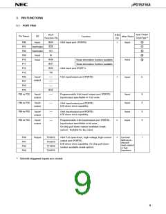
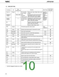
3.2 NON-PORT PINS
Input / Output
Dual-
Function
After Reset
Pin Name
T0 to T9
I/O
Circuit Type
*
Function Pin
Output
FIP controller/
driver output
pins.
Low level
(With an on-
chip pull-
down
resistor) or
high
impedance
(without a
pull-down
resistor)
–––
Digit output high-voltage high-current
output.
I
T10/S15 to
T13/S12
Digit/segment output dual-function
high-voltage high-current output.
Extra pins can be used as PORTH.
PH3 to PH0
Pull-down
resistor can be
incorporated in
bit-wise (mask
option).
T14/S11,
T15/S10
Digit/segment output dual-function
high-voltage high-current output.
Static output also possible.
–––
Segment output high voltage output.
Static output also possible.
S9
Segment high-voltage output.
S0 to S8
PPO
Output
Input
–––
Timer/pulse generator pulse output.
High
D
impedance
External event pulse input for timer/event counter.
Serial clock input/output.
TI0
SCK
SO
P13
P01
P02
P03
P00
B
F
Input
Input
Input
Input/output
Input/output
Serial data input pin or serial data input/output.
Serial data input or normal input.
G
SI
Input
Input
B
B
INT4
Edge-detected vectored interrupt input (rising and falling
edge detection).
Input
Edge-detected vectored interrupt input with noise
INT0
P10
B
elimination function (detection edge selection possible).
INT1
INT2
BUZ
P11
P12
P23
Input
Edge-detected testable input (rising edge detection).
B
E
Input
Input/output
Fixed frequency output (for buzzer or system clock
trimming).
Input
X1, X2
–––
Crystal/ceramic connect pin for main system clock
oscillation.
External clock input to X1 and its inverted clock input to
X2.
Crystal connect pin for subsystem clock oscillation.
External clock input to XT1 and XT2 open.
XT1
Input
–––
–––
XT2
System reset input (low level active).
FIP controller/driver output buffer power supply.
FIP controller/driver pull-down resistor connect pin.
Positive power supply.
Input
–––
–––
–––
–––
–––
RESET
VPRE
B
I
I
VLOAD
VDD
VSS
GND potential.
*
Schmitt-triggered inputs are circled.
10

 NEC [ NEC ]