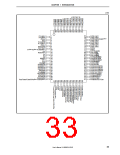
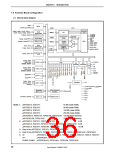
CHAPTER 1 INTRODUCTION
(2) Internal units
(a) CPU
The CPU uses five-stage pipeline control to enable single-clock execution of address calculations,
arithmetic logic operations, data transfers, and almost all other types of instruction processing.
Other dedicated on-chip hardware, such as a multiplier (16 bits × 16 bits → 32 bits) and a barrel shifter
(32 bits) help accelerate complex processing.
(b) Bus control unit (BCU)
The BCU starts a required external bus cycle based on the physical address obtained by the CPU.
When an instruction is fetched from external memory space and the CPU does not send a bus cycle start
request, the BCU generates a prefetch address and prefetches the instruction code. The prefetched
instruction code is stored in an internal instruction queue.
(c) ROM
This consists of a 256 KB, 128 KB, 96 KB, or 64 KB mask ROM or flash memory mapped to the address
spaces from 0000000H to 003FFFFH, 0000000H to 001FFFFH, 0000000H to 0017FFFH, or 0000000H to
000FFFFH, respectively.
ROM can be accessed by the CPU in one clock cycle during instruction fetch.
(d) RAM
This consists of a 16 KB, 6 KB, or 4 KB RAM mapped to the address spaces from 3FFB000H to
3FFEFFFH, 3FFD800H to 3FFEFFFH, or 3FFE000H to 3FFEFFFH.
RAM can be accessed by the CPU in one clock cycle during data access.
(e) Interrupt controller (INTC)
This controller handles hardware interrupt requests (NMI, INTP0 to INTP6) from on-chip peripheral
hardware and external hardware. Eight levels of interrupt priorities can be specified for these interrupt
requests, and multiplexed servicing control can be performed.
(f) Clock generator (CG)
A main clock oscillator and subclock oscillator are provided and generate the main clock oscillation
frequency (fX) and subclock frequency (fXT), respectively.
There are two modes: In the clock-through mode, fX is used as the main clock frequency (fXX) as is. In
the PLL mode, fX is used multiplied by 4.
The CPU clock frequency (fCPU) can be selected from among fXX, fXX/2, fXX/4, fXX/8, fXX/16, fXX/32, and fXT.
(g) Timer/counter
Four 16-bit timer/event counter 0 channels, one 16-bit timer/event counter P channelNote, and two 8-bit
timer/event counter 5 channels are incorporated, enabling measurement of pulse intervals and frequency
as well as programmable pulse output.
Two 8-bit timer/event counter 5 channels can be connected in cascade to configure a 16-bit timer.
Two 8-bit timer H channels enabling programmable pulse output are provided on chip.
Note µPD703215, 703215Y, 70F3215H, 70F3215HY only
37
User’s Manual U16890EJ1V0UD

 NEC [ NEC ]