CHAPTER 2 PIN FUNCTIONS
2.2 Pin Status
The address bus becomes undefined during accesses to the internal RAM and ROM. The data bus goes into the
high-impedance state without data output. The external bus control signal becomes inactive.
During peripheral I/O access, the address bus outputs the addresses of the on-chip peripheral I/Os that are
accessed. The data bus goes into the high-impedance state without data output. The external bus control signal
becomes inactive.
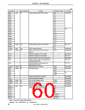
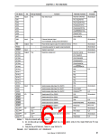
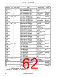
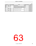
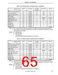
Table 2-2. Pin Operation Status in Operation Modes of V850ES/KF1
Operating Status
ResetNote 1
HALT Mode
IDLE Mode/
STOP Mode
Idle StateNote 2
Bus Hold
Pin
AD0 to AD15 (PDL0 to PDL15)
WAIT (PCM0)
Hi-Z
Hi-Z
Hi-Z
Hi-Z
Hi-Z
Hi-Z
Hi-Z
Hi-Z
Hi-Z
Operating
Operating
Operating
Operating
Operating
Operating
Operating
Operating
Operating
Hi-Z
–
Held
Hi-Z
–
–
CLKOUT (PCM1)
CS0, CS1 (PCS0, PCS1)
WR0, WR1 (PCT0, PCT1)
RD (PCT4)
L
Operating
Operating
Hi-Z
H
Held
H
H
Hi-Z
H
H
Hi-Z
ASTB (PCT6)
H
H
Hi-Z
HLDAK (PCM2)
H
H
L
HLDRQ (PCM3)
–
–
Operating
Notes 1. Since the bus control pin is also used as a port pin, it is initialized to the port mode (input) after reset.
2. The pin statuses in the idle state inserted after the T3 state are listed.
Remark Hi-Z: High impedance
H:
L:
–:
High-level output
Low-level output
Input without sampling (input acknowledgement not possible)
User’s Manual U15862EJ3V0UD
64

 NEC [ NEC ]