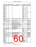
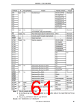
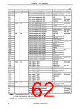
CHAPTER 2 PIN FUNCTIONS
(2/5)
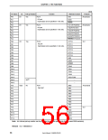
Products
Pin Name
ANI0
I/O
Pull-up Resistor
No
Function
Alternate Function
P70
Input
Analog voltage input for A/D converter
All products
ANI1
P71
ANI2
P72
ANI3
P73
ANI4
P74
ANI5
P75
ANI6
P76
ANI7
P77
ANI8
P78
KJ1
ANI9
P79
ANI10
ANI11
ANI12
ANI13
ANI14
ANI15
ANO0
ANO1
ASCK0
ASTB
P710
P711
P712
P713
P714
P715
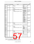
P10
KG1, KJ1
Output
Yes
Analog voltage output for D/A converter
UART0 serial clock input
P11
Input
Yes
No
P32
All products
All products
Output
Address strobe signal output for external
memory
PCT6
AVREF0
AVREF1
AVSS
–
–
–
–
–
–
–
–
Reference voltage for A/D converter
Reference voltage for D/A converter
Ground potential for A/D and D/A converters
–
–
–
–
All products
KG1, KJ1
All products
KG1, KJ1
BVDD
Positive power supply for bus interface and
alternate-function ports
KG1, KJ1
BVSS
–
–
Ground potential for bus interface and
alternate-function ports
–
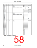
CLKOUT
CS0
Output
Output
No
No
Internal system clock output
Chip select output
PCM1
PCS0
PCS1
PCS2
PCS3
All products
All products
CS1
CS2
KJ1
CS3
EVDD
–
–
–
Positive power supply for external
Ground potential for external
Bus hold acknowledge output
Bus hold request input
–
–
All products
All products
All products
All products
All products
All products
EVSS
–
HLDAK
HLDRQ
ICNote
Output
Input
–
No
PCM2
PCM3
No
–
Internally connected
–
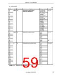
INTP0
INTP1
INTP2
INTP3
INTP4
INTP5
INTP6
Input
Yes
External interrupt request input
(maskable, analog noise elimination)
P03
P04
P05
P06
P913/A13
P914/A14
P915/A15
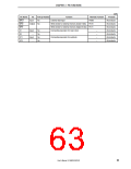
Note Only for the mask ROM versions
Remark KG1: V850ES/KG1, KJ1: V850ES/KJ1
User’s Manual U15862EJ3V0UD
60

 NEC [ NEC ]