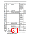
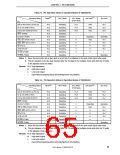
CHAPTER 2 PIN FUNCTIONS
(3/5)
Products
All products
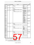
Pin Name
KR0
I/O
Pull-up Resistor
Yes
Function
Alternate Function
P50/TI011/RTP00
P51/TI50/RTP01
P52/TO50/RTP02
P53/SIA0/RTP03
P54/SOA0/RTP04
P55/SCKA0/RTP05
P90/A0/TXD1
Input
Key return input
KR1
KR2
KR3
KR4
KR5
KR6
KR7
P91/A1/RXD1
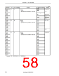
NMI
Input
Yes
External interrupt input
P02
All products
(non-maskable, analog noise elimination)
RD
Output
–
No
Read strobe signal output for external memory
Connecting capacitor for regulator output stabilization
System reset input
PCT4
All products
All products
All products
All products
REGC
RESET
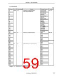
RTP00
RTP01
RTP02
RTP03
RTP04
RTP05
RTP10
RTP11
RTP12
RTP13
RTP14
RTP15
RXD0
–
–
Input
Output
–
–
Yes
Real-time output port
P50/TI011/KR0
P51/TI50/KR1
P52/TO50/KR2
P53/SIA0/KR3
P54/SOA0/KR4
P55/SCKA0/KR5
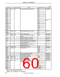
P60
KJ1
P61
P62
P63
P64
P65
Input
I/O
Yes
Yes
Serial receive data input for UART0
Serial receive data input for UART1
Serial receive data input for UART2
Serial clock I/O for CSI00
P31
All products
RXD1
P91/A1/KR7
P80/SDA1Note 1
P42
RXD2
KJ1
SCK00
SCK01
SCK02
SCKA0
SCKA1
SCL0Note 1
SCL1Note 3
SDA0Note 1
SDA1Note 3
All products
Serial clock I/O for CSI01
P99/A9
Serial clock I/O for CSI02
P68
KJ1
Serial clock I/O for CSIA0
P55/RTP05/KR5
P912/A12
P39
All products
KG1, KJ1
Serial clock I/O for CSIA1
I/O
I/O
NoNote 2
Yes
Serial clock I/O for I2C0, I2C1
All products
KJ1
P81/TXD2
P38
NoNote 2
Serial transmit/receive data I/O for I2C0, I2C1
All products
KJ1
Yes
P80/RXD2
Notes 1. Only for products with an I2C bus
2. An on-chip pull-up resistor can be provided by a mask option (only for the mask ROM and I2C bus
versions).
3. Only for the µPD703216Y, 703217Y, and 70F3217Y
Remark KG1: V850ES/KG1, KJ1: V850ES/KJ1
User’s Manual U15862EJ3V0UD
61

 NEC [ NEC ]