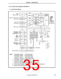
CHAPTER 1 INTRODUCTION
1.2 V850ES/KF1
1.2.1 Features (V850ES/KF1)
{ Number of instructions: 83
{ Minimum instruction execution time: 50 ns (operation at main clock (fXX) = 20 MHz)
{ General-purpose registers: 32 bits × 32 registers
{ Instruction set: Signed multiplication (16 × 16 → 32): 1 to 2 clocks
(Instructions without creating register hazards can be continuously executed in parallel)
Saturated operations (overflow and underflow detection functions are included)
32-bit shift instruction: 1 clock
Bit manipulation instructions
Load/store instructions with long/short format
{ Memory space: 64 MB of linear address space
Memory block division function: 2 MB, 64 KB (Total of 2 blocks)
{ External bus interface
16-bit data bus
{ Internal memory
µPD703208, 703208Y (Mask ROM: 64 KB/RAM: 4 KB)
µPD703209, 703209Y (Mask ROM: 96 KB/RAM: 4 KB)
µPD703210, 703210Y (Mask ROM: 128 KB/RAM: 6 KB)
µPD70F3210, 70F3210Y (Flash memory: 128 KB/RAM: 6 KB)
{ Interrupts and exceptions
Non-maskable interrupts: 3 sources
Maskable interrupts:
30 sources (µPD703208, 703209, 703210, 70F3210)
31 sources (µPD703208Y, 703209Y, 703210Y, 70F3210Y)
Software exceptions:
Exception trap:
Total: 67
32 sources
1 source
{ I/O lines:
{ Key interrupt function
{ Timer/counter
16-bit timer/event counter: 2 channels
8-bit timer/event counter: 2 channels
8-bit timer H: 2 channels
{ Watch timer: 1 channel
{ Watchdog timers
Watchdog timer 1 (also usable as oscillation stabilization timer): 1 channel
Watchdog timer 2: 1 channel
{ Serial interface (SIO)
Asynchronous serial interface (UART): 2 channels
3-wire serial I/O (CSI0): 2 channels
3-wire serial I/O (with automatic transmit/receive function) (CSIA): 1 channel
I2C bus interface (I2C): 1 channel
(µPD703208Y, 703209Y, 703210Y, 70F3210Y)
{ A/D converter: 10-bit resolution × 8 channels
{ Real-time output port: 6 bits × 1 channel
{ Power-save functions: HALT/IDLE/STOP modes, subclock/sub-IDLE modes
User’s Manual U15862EJ3V0UD
31

 NEC [ NEC ]