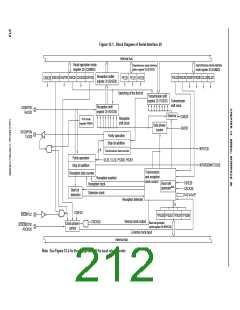
Figure 12-1. Block Diagram of Serial Interface 20
Internal bus
Serial operation mode
register 20 (CSIM20)
Asynchronous serial interface
status register 20 (ASIS20)
Asynchronous serial interface
mode register 20 (ASIM20)
Reception buffer
register 20 (RXB20)
TXE20 RXE20 PS201 PS200 CL20 SL20
CSIE20 SSE20 DAP20 DIR20 CSCK20 CKP20
PE20 FE20 OVE20
Switching of the first bit
Transmission shift
register 20 (TXS20) Transmission
shift clock
Reception shift
register 20 (RXS20)
SI20/P25/
RxD20
Selector
CSIE20
DAP20
Reception
shift clock
Port mode
register (PM24)
Data phase
control
SO20/P24/
TxD20
Parity operation
Stop bit addition
INTST20
4
Transmission data counter
Parity operation
Stop bit addition
SL20, CL20, PS200, PS201
INTSR20/INTCSI20
Transmission
and reception
clock control
Reception data counter
Reception enabled
CSIE20
CSCK20
/2 to f
/28
Baud rate
generatorNote
Reception clock
Start bit
detection
Detection clock
f
X
X
Reception detected
4
CSIE20
SS20/P22
TPS203
TPS202 TPS201 TPS200
Internal clock output
CSCK20
Baud rate generator
control register 20 (BRGC20)
Clock phase
control
SCK20/P23/
ASCK20
External clock input
Internal bus
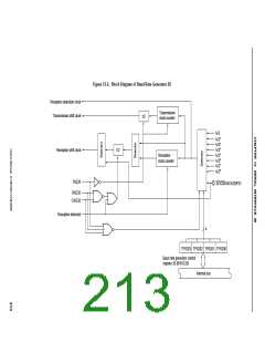
Note See Figure 12-2 for the configuration of the baud rate generator.

 NEC [ NEC ]