DDR3(L) 4Gb SDRAM
NT5CB(C)512M8DN / NT5CB(C)256M16DP
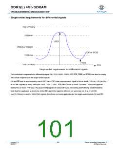
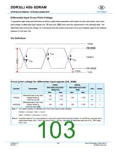
Differential Input Cross Point Voltage
To guarantee tight setup and hold times as well as output skew parameters with respect to clock and strobe, each cross
point voltage of differential input signals (CK, and DQS, ) must meet the requirements in the following table. The
differential input cross point voltage Vix is measured from the actual cross point of true and complete signal to the midlevel
between of VDD and VSS.
Vix Definition
VDD
,
VIX
VDD/2
VIX
VIX
CK,DQS
VSEL
VSS
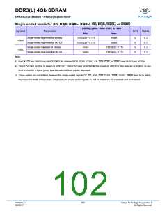
Cross point voltage for differential input signals (CK, DQS)
DDR3
DDR3L
800/1066/1333/1600/
1866/2133
800/1066/1333/1600/
1866
Symbol
Parameter
Unit
Notes
Min
Max
Min
Max
Differential Input Cross Point
Voltage relative to
- 150
+ 150
mV
mV
1
2
VIX(CK)
- 150
+ 150
- 175
- 150
+ 175
+ 150
VDD/2 for CK,
Differential Input Cross Point
Voltage relative to
VIX(DQS)
- 150
+ 150
mV
1
VDD/2 for DQS,
Note 1 The relation between Vix Min/Max and VSEL/VSEH should satisfy following:
(VDD/2) + VIX (min) - VSEL >= 25 mV ;
VSEH - ((VDD/2) + VIX (max)) >= 25 mV;
Note 2 Extended range for Vix is only allowed for clock and if single-ended clock input signals CK and are monotonic with a
single-ended swing VSEL / VSEH of at least VDD/2 +/-250 mV, and when the differential slew rate of CK - is larger
than 3 V/ns.
Version 2.3
02/2017
103
Nanya Technology Cooperation ©
All Rights Reserved.

 NANYA [ Nanya Technology Corporation. ]