NTC Proprietary
Level: Property
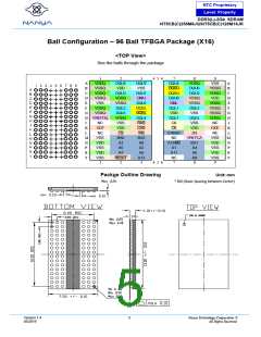
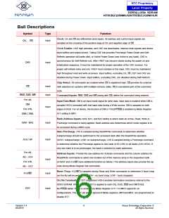
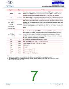
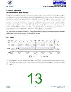
DDR3(L)-2Gb SDRAM
NT5CB(C)256M8JQ/NT5CB(C)128M16JR
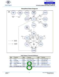
Basic Functionality
The DDR3(L) SDRAM is a high-speed dynamic random access memory internally configured as an eight-bank DRAM.
The DDR3(L) SDRAM uses an 8n prefetch architecture to achieve high speed operation. The 8n prefetch architecture is
combined with an interface designed to transfer two data words per clock cycle at the I/O pins. A single read or write
operation for the DDR3(L) SDRAM consists of a single 8n-bit wide, four clock data transfer at the internal DRAM core and
eight corresponding n-bit wide, one-half clock cycle data transfers at the I/O pins.
Read and write operation to the DDR3(L) SDRAM are burst oriented, start at a selected location, and continue for a burst
length of eight or a ‘chopped’ burst of four in a programmed sequence. Operation begins with the registration of an Active
command, which is then followed by a Read or Write command. The address bits registered coincident with the Active
command are used to select the bank and row to be activated (BA0-BA2 select the bank; A0-A14 select the row). The
address bit registered coincident with the Read or Write command are used to select the starting column location for the
burst operation, determine if the auto precharge command is to be issued (via A10), and select BC4 or BL8 mode ‘on the
fly’ (via A12) if enabled in the mode register.
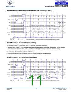
Prior to normal operation, the DDR3(L) SDRAM must be powered up and initialized in a predefined manner. The following
sections provide detailed information covering device reset and initialization, register definition, command descriptions and
device operation.
RESET and Initialization Procedure
Power-up Initialization sequence
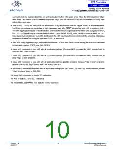
The Following sequence is required for POWER UP and Initialization
1. Apply power (REET is recommended to be maintained below 0.2 x VDD, all other inputs may be undefined). REET
needs to be maintained for minimum 200μs with stable power. CKE is pulled “Low” anytime before REETbeing de-
asserted (min. time 10ns). The power voltage ramp time between 300mV to VDDmin must be no greater than 200ms;
and during the ramp, VDD>VDDQ and (VDD-VDDQ) <0.3 Volts.
- VDD and VDDQ are driven from a single power converter output, AND
- The voltage levels on all pins other than VDD, VDDQ, VSS, VSSQ must be less than or equal to VDDQ and VDD on one
side and must be larger than or equal to VSSQ and VSS on the other side. In addition, VTT is limited to 0.95V max once
power ramp is finished, AND
- Vref tracks VDDQ/2.
OR
- Apply VDD without any slope reversal before or at the same time as VDDQ.
- Apply VDDQ without any slope reversal before or at the same time as VTT & Vref.
- The voltage levels on all pins other than VDD, VDDQ, VSS, VSSQ must be less than or equal to VDDQ and VDD on one
side and must be larger than or equal to VSSQ and VSS on the other side.
2. After REETis de-asserted, wait for another 500us until CKE become active. During this time, the DRAM will start
internal state initialization; this will be done independently of external clocks.
3. Clock (CK, ) need to be started and stabilized for at least 10ns or 5tCK (which is larger) before CKE goes active.
Since CKE is a synchronous signal, the corresponding set up time to clock (tIS) must be met. Also a NOP or Deselect
Version 1.4
05/2019
9
Nanya Technology Cooperation ©
All Rights Reserved.

 NANYA [ Nanya Technology Corporation. ]