NTC Proprietary
Level: Property
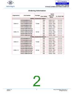
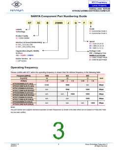
DDR3(L)-2Gb SDRAM
NT5CB(C)256M8JQ/NT5CB(C)128M16JR
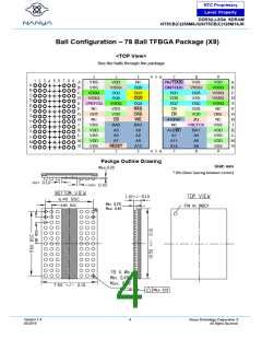
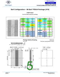
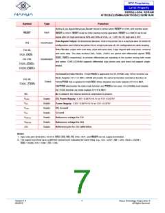
Ball Descriptions
Symbol
Type
Function
Clock: CK and are differential clock inputs. All address and control input signals are
sampled on the crossing of the positive edge of CK and negative edge of .
CK,
Input
Clock Enable: CKE high activates, and CKE low deactivates, internal clock signals and device
input buffers and output drivers. Taking CKE low provides Precharge Power-Down and Self-
Refresh operation (all banks idle), or Active Power-Down (row Active in any bank). CKE is
asynchronous for Self-Refresh exit. After VREF has become stable during the power on and
initialization sequence, it must be maintained for proper operation of the CKE receiver. For
proper self-refresh entry and exit, VREF must maintain to this input. CKE must be maintained
high throughout read and write accesses. Input buffers, excluding CK, , ODT and CKE are
disabled during Power Down. Input buffers, excluding CKE, are disabled during Self-Refresh.
CKE
Input
Chip Select: All commands are masked when is registered high. provides for external
rank selection on systems with multiple memory ranks. is considered part of the command
code.
Input
Input
RA, A, WE
For x8,
Command Inputs: RA, A and WE (along with ) define the command being entered.
Input Data Mask: DM is an input mask signal for write data. Input data is masked when DM is
sampled HIGH coincident with that input data during a Write access. DM is sampled on both
edges of DQS. For x8 device, the function of DM or TDQS/T is enabled by Mode Register
A11 setting in MR1.
DM
Input
Input
For x16,
DMU, DML
Bank Address Inputs: BA0, BA1, and BA2 define to which bank an Active, Read, Write or
Precharge command is being applied. Bank address also determines which mode register is to
be accessed during a MRS cycle.
BA0 - BA2
Auto-Precharge: A10 is sampled during Read/Write commands to determine whether
Autoprecharge should be performed to the accessed bank after the Read/Write operation.
(HIGH: Autoprecharge; LOW: no Autoprecharge). A10 is sampled during a Precharge command
to determine whether the Precharge applies to one bank (A10 LOW) or all banks (A10 HIGH). If
only one bank is to be precharged, the bank is selected by bank addresses.
A10 / AP
Input
For x8,
A0 – A14
For x16,
A0 – A13
Address Inputs: Provide the row address for Activate commands and the column address for
Read/Write commands to select one location out of the memory array in the respective bank.
(A10/AP and A12/ have additional function as below.) The address inputs also provide the op-
code during Mode Register Set commands.
Input
Burst Chop: A12/is sampled during Read and Write commands to determine if burst chop
A12/
Input
(on the fly) will be performed. (HIGH - no burst chop; LOW - burst chopped).
On Die Termination: ODT (registered HIGH) enables termination resistance internal to the
DDR3 SDRAM. When enabled, ODT is applied to each DQ, DQS, and DM/TDQS,
NU/T (when TDQS is enabled via Mode Register A11=1 in MR1) signal for x8
configurations. The ODT pin will be ignored if Mode-registers, MR1and MR2, are programmed to
disable RTT.
ODT
Input
Version 1.4
05/2019
6
Nanya Technology Cooperation ©
All Rights Reserved.

 NANYA [ Nanya Technology Corporation. ]