NTC Proprietary
Level: Property
DDR3(L)-2Gb SDRAM
NT5CB(C)256M8JQ/NT5CB(C)128M16JR
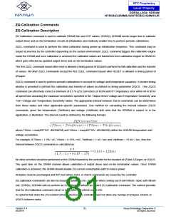
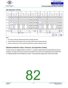
ZQ Calibration Timing
T0
T1
Ta0
Ta1
Ta2
Ta3
Tb0
Tb1
Tc0
Tc1
Tc2
CK
CK
CMD
ZQCL
NOP
NOP
NOP
Valid
Valid
Valid
Valid
Valid
Valid
Valid
ZQCS
NOP
NOP
NOP
Valid
Address
A10
Valid
Valid
Valid
Valid
CKE
ODT
(1)
(2)
Valid
(1)
(2)
Valid
DQ Bus
Activities
(3)
Hi-Z
tZQinit or tZQoper
Activities
(3)
Hi-Z
tZQCS
Do not
care
Time
Break
Note:
1. CKE must be continuously registered high during the calibration procedure.
2. On-die termination must be disabled via the ODT signal or MRS during the calibration procedure.
3. All devices connected to the DQ bus should be high impedance during the calibration procedure.
ZQ External Resistor Value, Tolerance, and Capacitive loading
In order to use the ZQ calibration function, a 240 ohm +/- 1% tolerance external resistor connected between the ZQ pin
and ground. The single resistor can be used for each SDRAM or one resistor can be shared between two SDRAMs if the
ZQ calibration timings for each SDRAM do not overlap. The total capacitive loading on the ZQ pin must be limited.
Version 1.4
05/2019
82
Nanya Technology Cooperation ©
All Rights Reserved.

 NANYA [ Nanya Technology Corporation. ]