NTC Proprietary
Level: Property
DDR3(L)-2Gb SDRAM
NT5CB(C)256M8JQ/NT5CB(C)128M16JR
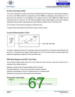
Synchronous ODT Mode
Synchronous ODT mode is selected whenever the DLL is turned on and locked. Based on the power-down definition,
these modes are:
Any bank active with CKE high
Refresh with CKE high
Idle mode with CKE high
Active power down mode (regardless of MR0 bit A12)
Precharge power down mode if DLL is enabled during precharge power down by MR0 bit A12
The direct ODT feature is not supported during DLL-off mode. The on-die termination resistors must be disabled by
continuously registering the ODT pin low and/or by programming the RTT_Nom bits MR1{A9,A6,A2} to {0,0,0} via a mode
register set command during DLL-off mode.
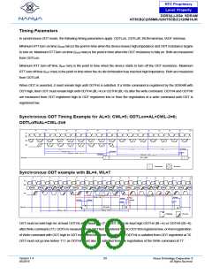
In synchronous ODT mode, RTT will be turned on ODTLon clock cycles after ODT is sampled high by a rising clock edge
and turned off ODTLoff clock cycles after ODT is registered low by a rising clock edge. The ODT latency is tied to the write
latency (WL) by: ODTLonn = WL - 2; ODTLoff = WL-2.
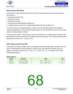
ODT Latency and Posted ODT
In synchronous ODT Mode, the Additive Latency (AL) programmed into the Mode Register (MR1) also applies to the ODT
signal. The DRAM internal ODT signal is delayed for a number of clock cycles defined by the Additive Latency (AL)
relative to the external ODT signal. ODTLon = CWL + AL - 2; ODTLoff = CWL + AL - 2. For details, refer to DDR3(L)
SDRAM latency definitions.
ODT Latency
Symbol
ODTLon
ODTLoff
Parameter
DDR3
Unit
tCK
ODT turn on Latency
ODT turn off Latency
WL - 2 = CWL + AL - 2
WL - 2 = CWL + AL - 2
tCK
Version 1.4
05/2019
68
Nanya Technology Cooperation ©
All Rights Reserved.

 NANYA [ Nanya Technology Corporation. ]