NTC Proprietary
Level: Property
DDR3(L)-2Gb SDRAM
NT5CB(C)256M8JQ/NT5CB(C)128M16JR
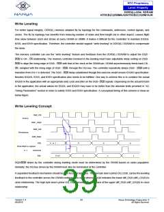
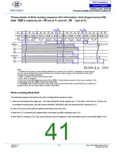
Timing details of Write leveling sequence (For Information. Only Support prime DQ)
DQS - is capturing CK - low at T1 and CK - high at T2
T1
tWLH
T2
tWLH
tWLS
tWLS
CK
CK
CMD
MRS
NOP
NOP
NOP
NOP
NOP
NOP
NOP
NOP
NOP
NOP
NOP
tMOD
ODT
tDQSL
tDQSH
tDQSL
tDQSH
tWLDQSEN
Diff_DQS
tWLMRD
tWLO
One Prime DQ:
Prime DQ
tWLO
tWLO
Late
Re ma ining
DQs
Early
Re ma ining
DQs
tWLO
tWLO
tWLOE
All DQs are Prime:
tWLMRD
tWLO
tWLO
Late
Re ma ining
DQs
tWLOE
Early
Re ma ining
DQs
tWLOE
tWLO
Undefined
Driving Mode
Do not
Care
Time
break
Note:
1. DRAM has the option to drive leveling feedback on a prime DQ or all DQs. If feedback is driven only on
one DQ, the remaining DQs must be driven low as shown in above Figure, and maintained at this state
through out the leveling procedure.
2. MRS: Load MR1 to enter write leveling mode
3. NOP: NOP or deselect
4. diff_DQS is the differential data strobe (DQS, ). Timing reference points are the zero crossings. DQS
is shown with solid line, is shown with dotted line.
6. DQS/ needs to fulfill minimum pulse width requirements tDQSH(min) and tDQSL(min) as defined for
regular Writes; the max pulse width is system dependent.
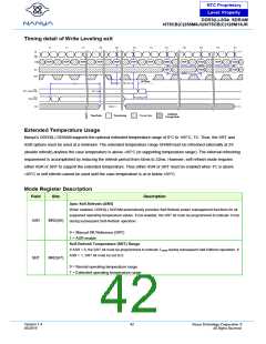
Write Leveling Mode Exit
The following sequence describes how Write Leveling Mode should be exited:
1. After the last rising strobe edge (see ~T0), stop driving the strobe signals (see ~Tc0). Note: From now on, DQ pins are
in undefined driving mode, and will remain undefined, until tMOD after the respective MR command (Te1).
2. Drive ODT pin low (tIS must be satisfied) and keep it low (see Tb0).
3. After the RTT is switched off, disable Write Level Mode via MRS command (see Tc2).
4. After tMOD is satisfied (Te1), any valid command may be registered. (MR commands may be issued after tMRD (Td1).
Version 1.4
05/2019
41
Nanya Technology Cooperation ©
All Rights Reserved.

 NANYA [ Nanya Technology Corporation. ]