NTC Proprietary
Level: Property
DDR3(L)-2Gb SDRAM
NT5CB(C)256M8JQ/NT5CB(C)128M16JR
Write Leveling
For better signal integrity, DDR3(L) memory adopted fly by topology for the commands, addresses, control signals, and
clocks. The fly by topology has benefits from reducing number of stubs and their length but in other aspect, causes flight
time skew between clock and strobe at every DRAM on DIMM. It makes it difficult for the Controller to maintain tDQSS,
tDSS, and tDSH specification. Therefore, the controller should support “write leveling” in DDR3(L) SDRAM to compensate
the skew.
The memory controller can use the “write leveling” feature and feedback from the DDR3(L) SDRAM to adjust the DQS -
to CK - relationship. The memory controller involved in the leveling must have adjustable delay setting on DQS -
to align the rising edge of DQS - with that of the clock at the DRAM pin. DRAM asynchronously feeds back CK -
, sampled with the rising edge of DQS - , through the DQ bus. The controller repeatedly delays DQS - until a
transition from 0 to 1 is detected. The DQS - delay established though this exercise would ensure tDQSS specification.
Besides tDQSS, tDSS, and tDSH specification also needs to be fulfilled. One way to achieve this is to combine the actual
tDQSS in the application with an appropriate duty cycle and jitter on the DQS- signals. Depending on the actual tDQSS
in the application, the actual values for tDQSL and tDQSH may have to be better than the absolute limits provided in “AC
Timing Parameters” section in order to satisfy tDSS and tDSH specification. A conceptual timing of this scheme is show as
below figure.
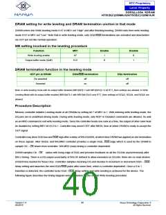
Write Leveling Concept
Diff_CK
Source
Diff _DQS
_
Diff CK
Destination
Diff_DQS
DQ
0 or 1
0
0
0
Push DQS to capture
0 -1 transition
DQ
0 or 1
1
1
1
DQS/ driven by the controller during leveling mode must be determined by the DRAM based on ranks populated.
Similarly, the DQ bus driven by the DRAM must also be terminated at the controller.
A separated feedback mechanism should be able for each byte lane. The low byte lane’s prime DQ, DQ0, carries the leveling
feedback to the controller across the DRAM configurations x4/x8 whereas DQ0 indicates the lower diff_DQS (diff_LDQS) to
clock relationship. The high byte lane’s prime DQ, DQ8, provides the feedback of the upper diff_DQS (diff_UDQS) to clock
relationship
Version 1.4
05/2019
39
Nanya Technology Cooperation ©
All Rights Reserved.

 NANYA [ Nanya Technology Corporation. ]