NTC Proprietary
Level: Property
DDR3(L)-2Gb SDRAM
NT5CB(C)256M8JQ/NT5CB(C)128M16JR
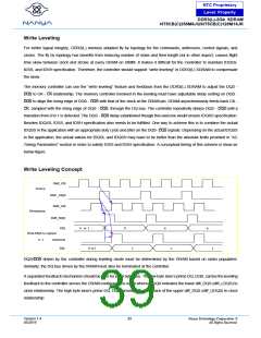
DRAM setting for write leveling and DRAM termination unction in that mode
DRAM enters into Write leveling mode if A7 in MR1 set “High” and after finishing leveling, DRAM exits from write leveling
mode if A7 in MR1 set “Low”. Note that in write leveling mode, only DQS/ terminations are activated and deactivated
via ODT pin not like normal operation.
MR setting involved in the leveling procedure
Function
MR1
Enable
Disable
Write leveling enable
Output buffer mode (Qoff)
A7
1
0
0
1
A12
DRAM termination function in the leveling mode
ODT pin at DRAM
DQS/ termination
DQs termination
De-asserted
off
on
off
off
Asserted
Note: In write leveling mode with its output buffer disabled (MR1[bit7]=1 with MR1[bit12]=1) all RTT_Nom settings are allowed; in Write
Leveling Mode with its output buffer enabled (MR1[bit7]=1 with MR1[bit12]=0) only RTT_Nom settings of RZQ/2, RZQ/4, and RZQ/6 are
allowed.
Procedure Description
Memory controller initiates Leveling mode of all DRAMs by setting bit 7 of MR1 to 1. With entering write leveling mode, the
DQ pins are in undefined driving mode. During write leveling mode, only NOP or Deselect commands are allowed. As well
as an MRS command to exit write leveling mode. Since the controller levels one rank at a time, the output of other rank must
be disabled by setting MR1 bit A12 to 1. Controller may assert ODT after tMOD, time at which DRAM is ready to accept the
ODT signal.
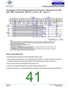
Controller may drive DQS low and high after a delay of tWLDQSEN, at which time DRAM has applied on-die termination
on these signals. After tDQSL and tWLMRD controller provides a single DQS, edge which is used by the DRAM to
sample CK – driven from controller. tWLMRD (max) timing is controller dependent.
DRAM samples CK - status with rising edge of DQS and provides feedback on all the DQ bits asynchronously after
tWLO timing. There is a DQ output uncertainty of tWLOE defined to allow mismatch on DQ bits; there are no read strobes
(DQS/DQS) needed for these DQs. Controller samples incoming DQ and decides to increment or decrement DQS –
delay setting and launches the next DQS/ pulse after some time, which is controller dependent. Once a 0 to 1
transition is detected, the controller locks DQS – delay setting and write leveling is achieved for the device. The
following figure describes the timing diagram and parameters for the overall Write leveling procedure.
Version 1.4
05/2019
40
Nanya Technology Cooperation ©
All Rights Reserved.

 NANYA [ Nanya Technology Corporation. ]