NTC Proprietary
Level: Property
DDR3(L)-2Gb SDRAM
NT5CB(C)256M8JQ/NT5CB(C)128M16JR
Input Clock frequency change
Once the DDR3(L) SDRAM is initialized, the DDR3(L) SDRAM requires the clock to be “stable” during almost all states of
normal operation. This means once the clock frequency has been set and is to be in the “stable state”, the clock period is
not allowed to deviate except for what is allowed for by the clock jitter and SSC (spread spectrum clocking) specification.
The input clock frequency can be changed from one stable clock rate to another stable clock rate under two conditions: (1)
Self-Refresh mode and (2) Precharge Power-Down mode. Outside of these two modes, it is illegal to change the clock
frequency.
For the first condition, once the DDR3(L) SDRAM has been successfully placed in to Self-Refresh mode and tCKSRE has
been satisfied, the state of the clock becomes a don’t care. Once a don’t care, changing the clock frequency is permissible,
provided the new clock frequency is stable prior to tCKSRX. When entering and exiting Self-Refresh mode of the sole
purpose of changing the clock frequency. The DDR3(L) SDRAM input clock frequency is allowed to change only within the
minimum and maximum operating frequency specified for the particular speed grade.
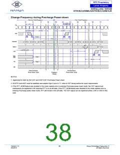
The second condition is when the DDR3(L) SDRAM is in Precharge Power-Down mode (either fast exit mode or slow exit
mode). If the RTT_Nom feature was enabled in the mode register prior to entering Precharge power down mode, the ODT
signal must continuously be registered LOW ensuring RTT is in an off state. If the RTT_Nom feature was disabled in the
mode register prior to entering Precharge power down mode, RTT will remain in the off state. The ODT signal can be
registered either LOW or HIGH in this case. A minimum of tCKSRE must occur after CKE goes LOW before the clock
frequency may change. The DDR3(L) SDRAM input clock frequency is allowed to change only within the minimum and
maximum operating frequency specified for the particular speed grade. During the input clock frequency change, ODT and
CKE must be held at stable LOW levels. Once the input clock frequency is changed, stable new clocks must be provided to
the DRAM tCKSRX before precharge Power Down may be exited; after Precharge Power Down is exited and tXP has
expired, the DLL must be RESET via MRS. Depending on the new clock frequency additional MRS commands may need
to be issued to appropriately set the WR, CL, and CWL with CKE continuously registered high. During DLL re-lock period,
ODT must remain LOW and CKE must remain HIGH. After the DLL lock time, the DRAM is ready to operate with new clock
frequency.
Version 1.4
05/2019
37
Nanya Technology Cooperation ©
All Rights Reserved.

 NANYA [ Nanya Technology Corporation. ]