NTC Proprietary
Level: Property
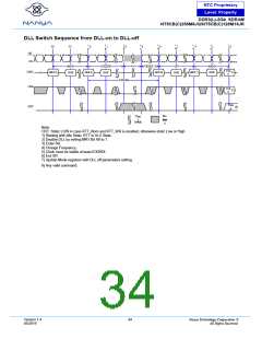
DDR3(L)-2Gb SDRAM
NT5CB(C)256M8JQ/NT5CB(C)128M16JR
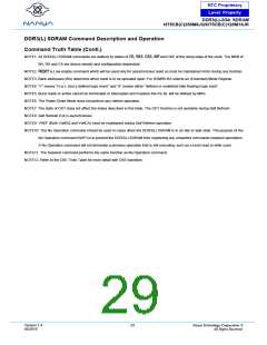
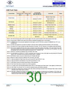
CKE Truth Table
CKE
Command (N)
Current State
Action (N)
Notes
Previous Cycle Current Cycle
RA, A,WE,
(N-1)
(N)
X
L
L
Maintain Power-Down
Power-Down Exit
14,15
11,14
Power-Down
Self-Refresh
L
H
L
DESELECT or NOP
X
L
Maintain Self-Refresh
Self-Refresh Exit
15,16
L
H
L
DESELECT or NOP
DESELECT or NOP
DESELECT or NOP
DESELECT or NOP
DESELECT or NOP
DESELECT or NOP
DESELECT or NOP
REFRESH
8,12,16
Bank(s) Active
Reading
H
Active Power-Down Entry
Power-Down Entry
11,13,14
11,13,14,17
11,13,14,17
11,13,14,17
11
H
L
Writing
H
L
Power-Down Entry
Precharging
Refreshing
H
L
Power-Down Entry
H
L
Precharge Power-Down Entry
Precharge Power-Down Entry
Self-Refresh
H
L
11,13,14,18
9,13,18
All Banks Idle
H
L
NOTE 1 CKE (N) is the logic state of CKE at clock edge N; CKE (N-1) was the state of CKE at the previous clock edge.
NOTE 2 Current state is defined as the state of the DDR3(L) SDRAM immediately prior to clock edge N.
NOTE 3 COMMAND (N) is the command registered at clock edge N, and ACTION (N) is a result of COMMAND (N), ODT is not
included here.
NOTE 4 All states and sequences not shown are illegal or reserved unless explicitly described elsewhere in this document.
NOTE 5 The state of ODT does not affect the states described in this table. The ODT function is not available during Self-Refresh.
NOTE 6 CKE must be registered with the same value on tCKEmin consecutive positive clock edges. CKE must remain at the valid
input level the entire time it takes to achieve the tCKEmin clocks of registrations. Thus, after any CKE transition, CKE may
not transition from its valid level during the time period of tIS + tCKEmin + tIH.
NOTE 7 DESELECT and NOP are defined in the Command Truth Table.
NOTE 8 On Self-Refresh Exit DESELECT or NOP commands must be issued on every clock edge occurring during the tXS period.
Read or ODT commands may be issued only after tXSDLL is satisfied.
NOTE 9 Self-Refresh modes can only be entered from the All Banks Idle state.
NOTE 10 Must be a legal command as defined in the Command Truth Table.
NOTE 11 Valid commands for Power-Down Entry and Exit are NOP and DESELECT only.
NOTE 12 Valid commands for Self-Refresh Exit are NOP and DESELECT only.
NOTE 13 Self-Refresh cannot be entered during Read or Write operations.
NOTE 14 The Power-Down does not perform any refresh operations.
NOTE 15 “X” means “don’t care“(including floating around VREF) in Self-Refresh and Power-Down. It also applies to Address pins.
NOTE 16 VREF (Both Vref_DQ and Vref_CA) must be maintained during Self-Refresh operation.
NOTE 17 If all banks are closed at the conclusion of the read, write or precharge command, then Precharge Power-Down is entered,
otherwise Active Power-Down is entered.
NOTE 18 ‘Idle state’ is defined as all banks are closed (tRP, tDAL, etc. satisfied), no data bursts are in progress, CKE is high, and
all timings from previous operations are satisfied (tMRD, tMOD, tRFC, tZQinit, tZQoper, tZQCS, etc.) as well as all Self-
Refresh exit and Power-Down Exit parameters are satisfied (tXS, tXP, tXPDLL, etc).
Version 1.4
05/2019
30
Nanya Technology Cooperation ©
All Rights Reserved.

 NANYA [ Nanya Technology Corporation. ]