NTC Proprietary
Level: Property
DDR3(L)-2Gb SDRAM
NT5CB(C)256M8JQ/NT5CB(C)128M16JR
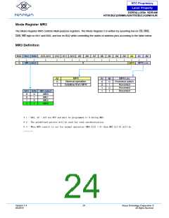
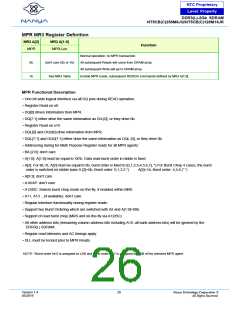
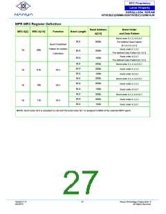
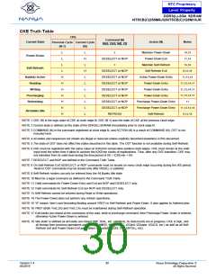
MPR MR3 Register Definition
MR3 A[2]
MR3 A[1:0]
Function
MPR
MPR-Loc
Normal operation, no MPR transaction.
0b
1b
don't care (0b or 1b)
See MR3 Table
All subsequent Reads will come from DRAM array.
All subsequent Write will go to DRAM array.
Enable MPR mode, subsequent RD/RDA commands defined by MR3 A[1:0].
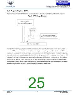
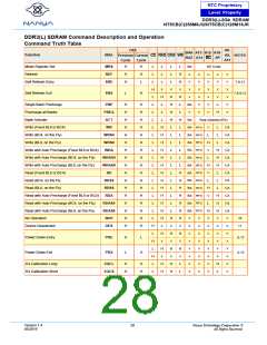
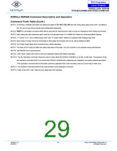
MPR Functional Description
• One bit wide logical interface via all DQ pins during READ operation.
• Register Read on x8:
• DQ[0] drives information from MPR.
• DQ[7:1] either drive the same information as DQ [0], or they drive 0b.
• Register Read on x16:
• DQL[0] and DQU[0] drive information from MPR.
• DQL[7:1] and DQU[7:1] either drive the same information as DQL [0], or they drive 0b.
• Addressing during for Multi Purpose Register reads for all MPR agents:
• BA [2:0]: don’t care
• A[1:0]: A[1:0] must be equal to ‘00’b. Data read burst order in nibble is fixed
• A[2]: For BL=8, A[2] must be equal to 0b, burst order is fixed to [0,1,2,3,4,5,6,7], *) For Burst Chop 4 cases, the burst
order is switched on nibble base A [2]=0b, Burst order: 0,1,2,3 *)
A[2]=1b, Burst order: 4,5,6,7 *)
• A[9:3]: don’t care
• A10/AP: don’t care
• A12/BC: Selects burst chop mode on-the-fly, if enabled within MR0.
• A11, A13... (if available): don’t care
• Regular interface functionality during register reads:
• Support two Burst Ordering which are switched with A2 and A[1:0]=00b.
• Support of read burst chop (MRS and on-the-fly via A12/BC)
• All other address bits (remaining column address bits including A10, all bank address bits) will be ignored by the
DDR3(L) SDRAM.
• Regular read latencies and AC timings apply.
• DLL must be locked prior to MPR Reads.
NOTE: *Burst order bit 0 is assigned to LSB and burst order bit 7 is assigned to MSB of the selected MPR agent.
Version 1.4
05/2019
26
Nanya Technology Cooperation ©
All Rights Reserved.

 NANYA [ Nanya Technology Corporation. ]