• This PDF catalog is downloaded from the website of Murata Manufacturing co., ltd. Therefore, it’s specifications are subject to change or our products in it may be discontinued without advance notice. Please check with our
• Please read rating and !CAUTION (for storage, operating, rating, soldering, mounting and handling) in this catalog to prevent smoking and/or burning, etc.
!Note
!Note
C02E.pdf
sales representatives or product engineers before ordering.
• This catalog has only typical specifications because there is no space for detailed specifications. Therefore, please approve our product specifications or transact the approval sheet for product specifications before ordering0. 9.9.18
• This PDF catalog has only typical specifications because there is no space for detailed specifications. Therefore, please approve our product specifications or transact the approval sheet for product specifications before ordering.
Notice
Continued from the preceding page.
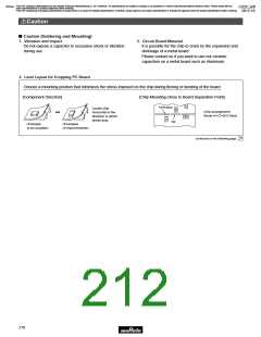
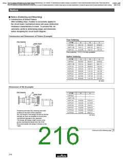
Land Layout to Prevent Excessive Solder
Mounting Close to a Chassis
Mounting with Leaded Components
Mounting Leaded Components Later
Soldering Iron
Lead Wire of
Component to be
Connected Later.
Lead Wire Connected
to a Part Provided
with Lead Wires.
d1
Chassis
Solder (Ground solder)
Examples of
Prohibition
Adhesive
Base board
Land Pattern
in section
in section
in section
d2
Solder Resist
d1<d2
Solder Resist
Examples of
Improvements
by the Land
Division
Solder Resist
in section
in section
in section
2. Mounting of Chips
Thickness of adhesives applied
Keep thickness of adhesives applied (50-105µm or more)
to reinforce the adhesive contact considering the
thickness of the termination or capacitor (20-70µm) and
the land pattern (30-35µm).
Mechanical shock of the chip placer
When the positioning claws and pick-up nozzle are worn,
the load is applied to the chip while positioning is
concentrated in one position, thus causing cracks,
breakage, faulty positioning accuracy, etc.
Careful checking and maintenance are necessary to
prevent unexpected trouble.
An excessively low bottom dead point of the suction
nozzle imposes great force on the chip during mounting,
causing cracked chips. Please set the suction nozzle's
bottom dead point on the upper surface of the board.
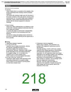
3. Soldering
(1) Limit of losing effective area of the terminations and
conditions needed for soldering.
(2) Flux Application
An excessive amount of flux generates a large quantity of
flux gas, causing deteriorated solderability. So apply flux
thinly and evenly throughout. (A foaming system is
generally used for flow soldering.)
Depending on the conditions of the soldering
temperature and/or immersion (melting time),
effective areas may be lost in some part of the
terminations.
Flux containing too high percentage of halide may cause
corrosion of the outer electrodes unless sufficient
cleaning. Use flux with a halide content of 0.2% max.
Do not use strong acidic flux.
To prevent this, be careful in soldering so that any
possible loss of the effective area on the terminations
will securely remain at a maximum of 25% on all
edge length A-B-C-D-A of part with A, B, C, D, shown
Do not use water-soluble flux*.
(*Water-soluble flux can be defined as non rosin type flux
including wash-type flux and non-wash-type flux.)
in the Figure below.
18
A
B
D
Termination
C
Continued on the following page.
215

 MURATA [ muRata ]