• This PDF catalog is downloaded from the website of Murata Manufacturing co., ltd. Therefore, it’s specifications are subject to change or our products in it may be discontinued without advance notice. Please check with our
• Please read rating and !CAUTION (for storage, operating, rating, soldering, mounting and handling) in this catalog to prevent smoking and/or burning, etc.
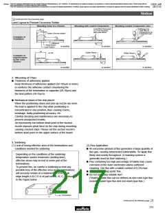
!Note
!Note
C02E.pdf
sales representatives or product engineers before ordering.
• This catalog has only typical specifications because there is no space for detailed specifications. Therefore, please approve our product specifications or transact the approval sheet for product specifications before ordering0. 9.9.18
• This PDF catalog has only typical specifications because there is no space for detailed specifications. Therefore, please approve our product specifications or transact the approval sheet for product specifications before ordering.
Notice
Notice (Soldering and Mounting)
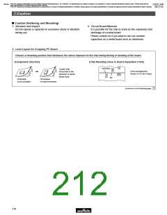
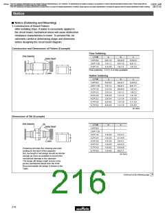
1. Construction of Board Pattern
After installing chips, if solder is excessively applied to
the circuit board, mechanical stress will cause destruction
resistance characteristics to lower. To prevent this, be
extremely careful in determining shape and dimension
before designing the circuit board diagram.
Construction and Dimensions of Pattern (Example)
Flow Soldering
Chip Capacitor
LgW
a
b
c
Solder Resist
1.6g0.8
2.0g1.25
3.2g1.6
0.6-1.0
1.0-1.2
2.2-2.6
0.8-0.9
0.9-1.0
1.0-1.1
0.6-0.8
0.8-1.1
1.0-1.4
c
L
W
Flow soldering : 3.2g1.6 or less available.
Land
b
a
Reflow Soldering
LgW
1.6g0.8
2.0g1.25
3.2g1.6
3.2g2.5
4.5g2.0
4.5g3.2
5.7g2.8
5.7g5.0
a
b
c
0.6-0.8
1.0-1.2
2.2-2.4
2.0-2.4
2.8-3.4
2.8-3.4
4.0-4.6
4.0-4.6
0.6-0.7
0.6-0.7
0.8-0.9
1.0-1.2
1.2-1.4
1.2-1.4
1.4-1.6
1.4-1.6
0.6-0.8
0.8-1.1
1.0-1.4
1.8-2.3
1.4-1.8
2.3-3.0
2.1-2.6
3.5-4.8
(in mm)
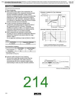
Dimensions of Slit (Example)
Chip Capacitor
Slit
Solder Resist
LgW
1.6g0.8
2.0g1.25
3.2g1.6
3.2g2.5
4.5g2.0
4.5g3.2
5.7g2.8
5.7g5.0
d
e
-
-
-
-
d
L
1.0-2.0
1.0-2.0
1.0-2.8
1.0-2.8
1.0-4.0
1.0-4.0
3.2-3.7
4.1-4.6
3.6-4.1
4.8-5.3
4.4-4.9
6.6-7.1
e
W
Land
Preparing slit helps flux cleaning and resin
coating on the back of the capacitor.
But, the length of slit design should be shorter
enough as much as possible to prevent the
mechanical damage in the capacitor.
The longer slit design might receive more
severe mechanical stress from the PCB.
Recommendable slit design is shown in the
Table.
(in mm)
Continued on the following page.
18
214

 MURATA [ muRata ]