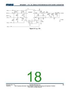
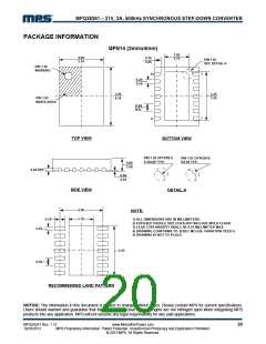
MPQ28261 – 21V, 3A, 500kHz SYNCHRONOUS STEP-DOWN CONVERTER
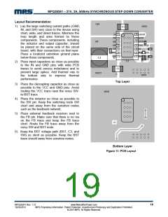
Layout Recommendation
VIN
SW
1) Lay the large switching current paths (GND,
IN, and SW) very close to the device using
short, wide, and direct traces. Minimize the
loop length and area formed by these
components. These components, including
the inductor and output capacitor, should
be placed on the same side of the circuit
board, with their connections on that layer.
Place a localized unbroken ground plane
below these components.
GND
C1
1
2
3
4
5
6
7
14
13
12
11
10
9
AGND
IN
SW
GND
GND
VCC
SS
SW
SW
C4
C7
R2
SW
R10
C3
BST
EN
PG
FB
8
Rt
L1
R1
U1
2) Place input capacitors as close as possible
to the IN and GND pins with wide PCB
traces to avoid excess inductance and to
prevent large spikes. Add thermal vias to
the bottom side to improve thermal
performance.
C2
VOUT
GND
Top Layer
3) Place the decoupling capacitor as close as
possible to the VCC and GND pins. Avoid
routing the VCC trace near the noisy SW-
to-BST trace.
GND
4) Place the inductor as close as possible to
the SW pin. Keep the switching node SW
short and away from the sensitive nodes
such as the feedback network.
5) Place external feedback resistors next to
the FB pin. Make sure that there is no via
on the FB trace and keep the FB trace
short. Route the FB trace away from the
noisy SW and BST node.
6) Keep the BST voltage path (BST, C3, and
SW) as short as possible. Keep the BST
trace should away from sensitive nodes.
Bottom Layer
Figure 11: PCB Layout
MPQ28261 Rev. 1.12
10/10/2013
www.MonolithicPower.com
MPS Proprietary Information. Patent Protected. Unauthorized Photocopy and Duplication Prohibited.
© 2013 MPS. All Rights Reserved.
19

 MPS [ MONOLITHIC POWER SYSTEMS ]