MPQ28261 – 21V, 3A, 500kHz SYNCHRONOUS STEP-DOWN CONVERTER
OPERATION
The
MPQ28261
is
a
high-frequency,
(RUP + RDOWN
)
V
= 1.4×
(V)
IN−START
synchronous, rectified, step-down, switch mode
converter with built-in internal power MOSFETs.
It offers a very compact solution to output a 3A
continuous output current over a wide input
supply range, with excellent load and line
regulation.
RDOWN
For example, for RUP=100kꢀ and RDOWN=51kꢀ,
the VIN-START is set at 4.15V.
To reduce noise, add a 10nF ceramic capacitor
from EN to GND.
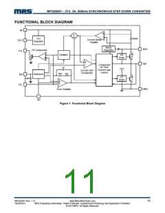
The MPQ28261 operates in a fixed-frequency
peak-current–control mode to regulate the
output voltage. Around the start of a PWM cycle,
the integrated high-side power MOSFET (HS-
FET) turns on and remains on until its current
reaches the value set by the COMP voltage.
When the power switch turns off, it remains off
until the next clock cycle starts. If the current in
the HS-FET does not reach the COMP set
value for 90% of one PWM period, the HS-FET
will turn off.
An internal zener diode on the EN pin clamps
the EN pin voltage to prevent run away. The
maximum pull up current assuming the worst
case 6V for the internal zener clamp should be
less than 0.2mA.
Therefore, when driving EN with an external
logic signal, use an EN voltage less than 6V.
When connecting EN to IN through a pull-up
resistor or a resistive voltage divider, select a
resistance that ensures a maximum pull-up
current less than 0.2mA.
Error Amplifier
If using a resistive voltage divider and VIN
exceeds 6V, then the minimum resistance for
the pull-up resistor RUP should meet:
The error amplifier compares VFB against the
internal 0.6V reference (VREF) and outputs a
current proportional to the difference. The
output current both charges and discharges the
internal compensation network to form the
COMP voltage, which controls the power
MOSFET current. The optimized internal
compensation network minimizes the external
component counts and simplifies the control
loop design.
V − 6V
RUP
6V
IN
−
≤ 0.2mA
RDOWN
With only RUP (the pull-down resistor, RDOWN, is
not connected), then the VCC UVLO threshold
determines VIN-START, so the minimum resistor
value is:
Internal Regulator
V − 6V
0.2mA
IN
The 5V regulator powers most of the internal
circuitry. This regulator takes the VIN input and
operates in the full VIN range When VIN exceeds
5.1V, the regulator outputs at its maximum level;
when VIN falls below 5.1V, the output decreases.
RUP
≥
(Ω)
Under-Voltage Lockout
Under-voltage lockout (UVLO) protects the chip
from operating at insufficient supply voltages.
The UVLO comparator monitors the output
voltage of the internal regulator, VCC. The
UVLO rising threshold is about 4.0V while its
falling threshold is 3.2V.
The regulator requires
capacitor for decoupling purposes.
a
0.1µF ceramic
Configuring the Enable Control
The MPQ28261 has a dedicated Enable control
pin (EN): pulling this pin high or low enables or
disables the IC. Tie EN to VIN through a resistor
for automatic start up. Choose the values of the
pull-up resistor (RUP from the IN pin to the EN
pin) and the pull-down resistor (RDOWN from the
EN pin to GND) to determine the automatic
start-up voltage:
Power Good Indicator
MPQ28261 uses the open drain of an NMOS
for the Power Good (PG) indicator. When VFB
rises above 90% of the reference voltage, PG
pin is pulled up to VCC by an external resistor
MPQ28261 Rev. 1.12
10/10/2013
www.MonolithicPower.com
MPS Proprietary Information. Patent Protected. Unauthorized Photocopy and Duplication Prohibited.
© 2013 MPS. All Rights Reserved.
12

 MPS [ MONOLITHIC POWER SYSTEMS ]