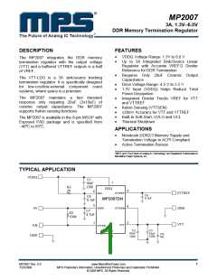
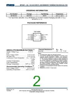
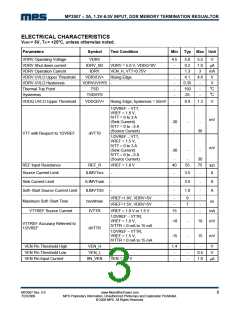
MP2007 – 3A, 1.3V-6.0V INPUT, DDR MEMORY TERMINATION REGUALTOR
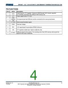
PIN FUNCTIONS
Pin #
Name
Description
Power input for VTT regulator. Connect to GND through 10uF ceramic capacitor.
It is normally connected to the VDDQ of DDR memory rail.
1
2
DDQ
VTT
Power output for the VTT LDO.
GND
3
Exposed The exposed pad and GND pin must be connected to the same ground plane.
Pad
4
5
VTTSEN
Kelvin sensed feedback signal.
VDRV
Chip bias Voltage.
6
7
8
REF
EN
LDO signal input for generating VDDQ/2 reference.
VTT regulator enable input. High to enable the chip.
Buffered output for the system. The receiving end of the DDR memory cells needs this
signal for their input comparator.
VTTREF
MP2007 Rev. 0.9
7/23/2009
www.MonolithicPower.com
MPS Proprietary Information. Unauthorized Photocopy and Duplication Prohibited.
© 2009 MPS. All Rights Reserved.
4

 MPS [ MONOLITHIC POWER SYSTEMS ]