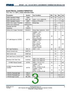
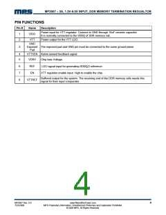
MP2007 – 3A, 1.3V-6.0V INPUT, DDR MEMORY TERMINATION REGUALTOR
Another power consumption is the current used
APPLICATION INFORMATION
for internal control circuitry from VDDQ supply.
This power needs to be effectively dissipated
from the package.
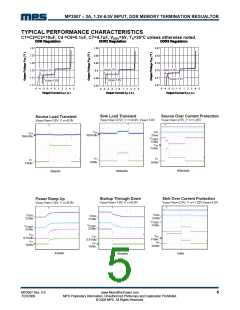
Input Capacitor
Depending on the trace impedance from the
power supply to the part, transient increase of
source current is supplied mostly by the charge
from the VDDQ input capacitor. Use a 10μF (or
more) ceramic capacitor to supply this transient
charge. Provide more input capacitance as more
output capacitance is used at VTT. In general,
use 1/2 COUT for input.
PCB Layout Guidelines
Good PCB layout design is critical to ensure high
performance and stable operation of the DDR
power controller. The following items must be
considered when preparing PCB layout:
1. All high−current traces must be kept as short
and wide as possible to reduce power loss.
Output Capacitor
For stable operation, total capacitance of the VTT
output terminal can be equal or greater than
20μF. Attach two 10μF ceramic capacitors in
parallel to minimize the effect of ESR and ESL. If
the ESR is greater than 10mΩ, insert an R-C
filter between the output and the VTTSEN input
to achieve loop stability. The R-C filter time
constant should be almost the same or slightly
lower than the time constant of the output
capacitor and its ESR.
High−current traces are the trace from the input
voltage terminal to VDDQ pin, the trace from the
VTT output terminal to the load, the trace from
the input ground terminal to the VTT output
ground terminal, and the trace from VTT output
ground terminal to the GND pin.
Power handling and heaksinking of high−current
traces can be improved by also routing the same
high−current traces in the other layers by the
same path and joining them together with
multiple vias.
VDRV Capacitor
Add a ceramic capacitor with a value between
1.0μF and 4.7μF placed close to the VDRV pin,
to stabilize 5V from any parasitic impedance from
the supply.
2. To ensure the proper function of the device,
separated ground connections should be used
for different parts of the application circuit
according to their functions.
Thermal design
The VTT output capacitor ground should be
connected to the GND pin first with a short trace,
it is then connected to the ground plane of GND.
The input capacitor ground, the VTT output
capacitor ground, the VDDQ decoupling
capacitor ground should be connected to the
GND plane.
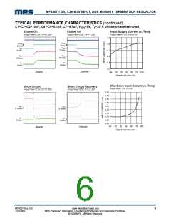
As the MP2007 is a linear regulator, the VTT
current flow in both source and sink directions
generate power dissipation from the device.
In the source phase, the potential difference
between VDDQ and VTT times VTT current
becomes
the
power
dissipation,
Psource=(VDDQ-VTT) x Isource
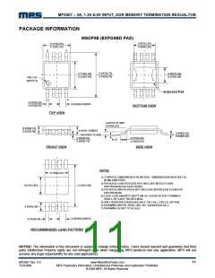
3. The thermal pad of the 8-pin MSOP package
should to be connected to GND for better thermal
performance. It is recommended to use a PCB
with 1 oz or 2oz copper foil.
In this case, if VDDQ is connected to an
alternative power supply lower than VDDQ
voltage, power loss can be decreased.
For the sink phase, VTT voltage is applied across
the internal LDO regulator, and the power
dissipation Psink is:
4. A separate sense trace should be used to
connect the VTT point of regulation, which is
usually the local bypass capacitor for load, to the
VTTSEN pin.
Psink=VTT x Isink
The device does not sink and source the current
at the same time and source/sink current varies
rapidly with time. The actual power dissipation to
be considered for thermal design is an average
of the above values over time.
5. Separate sense trace should be used to
connect the VREF point of regulation to the
VTTREF pin to ensure the accuracy of the
reference voltage to VTT.
MP2007 Rev. 0.2
7/23/2009
www.MonolithicPower.com
MPS Proprietary Information. Unauthorized Photocopy and Duplication Prohibited.
© 2009 MPS. All Rights Reserved.
9

 MPS [ MONOLITHIC POWER SYSTEMS ]