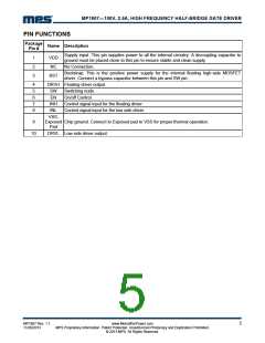
MP1907―100V, 2.5A, HIGH FREQUENCY HALF-BRIDGE GATE DRIVER
PIN FUNCTIONS
Package
Pin #
Name Description
Supply input. This pin supplies power to all the internal circuitry. A decoupling capacitor to
ground must be placed close to this pin to ensure stable and clean supply.
1
2
3
VDD
NC
No Connection.
Bootstrap. This is the positive power supply for the internal floating high-side MOSFET
driver. Connect a bypass capacitor between this pin and SW pin.
BST
4
5
6
7
8
DRVH Floating driver output.
SW
EN
Switching node.
On/off Control.
INH
INL
Control signal input for the floating driver.
Control signal input for the low side driver.
VSS,
9
Exposed Chip ground. Connect to Exposed pad to VSS for proper thermal operation.
Pad
10
DRVL Low side driver output.
MP1907 Rev. 1.1
11/20/2013
www.MonolithicPower.com
MPS Proprietary Information. Patent Protected. Unauthorized Photocopy and Duplication Prohibited.
© 2013 MPS. All Rights Reserved.
5

 MPS [ MONOLITHIC POWER SYSTEMS ]