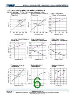
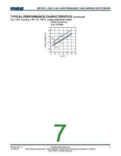
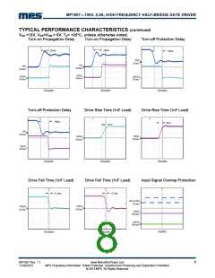
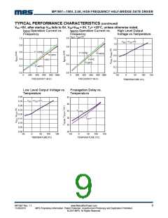
MP1907―100V, 2.5A, HIGH FREQUENCY HALF-BRIDGE GATE DRIVER
ORDERING INFORMATION
Part Number*
Package
Top Marking
MP1907GQ
QFN10 (3 x 3 mm)
ABN
* For Tape & Reel, add suffix –Z (e.g. MP1907GQ–Z);
PACKAGE REFERENCE
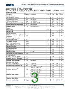
ABSOLUTE MAXIMUM RATINGS (1)
Thermal Resistance (5)
QFN10 (3x3)...........................50...... 12... °C/W
θJA
θJC
Supply Voltage (VDD).....................-0.3V to +20V
SW Voltage (VSW) .........................-5.0V to 105V
BST Voltage (VBST) .......................-0.3V to 110V
BST to SW....................................-0.3V to +18V
DRVH to SW.............. -0.3V to (BST-SW) +0.3V
DRVL to VSS...................... -0.3V to (VDD+0.3V)
All Other Pins..................................-0.3V to 20V
Notes:
1) Exceeding these ratings may damage the device.
2) The maximum allowable power dissipation is a function of the
maximum junction temperature TJ (MAX), the junction-to-
ambient thermal resistance θJA, and the ambient temperature
TA. The maximum allowable continuous power dissipation at
any ambient temperature is calculated by PD (MAX) = (TJ
(MAX)-TA)/θJA. Exceeding the maximum allowable power
dissipation will cause excessive die temperature, and the
regulator will go into thermal shutdown. Internal thermal
shutdown circuitry protects the device from permanent
damage.
(2)
Continuous Power Dissipation (TA =+25°C)
QFN10 (3x3).............................................. 2.5W
Junction Temperature...............................150°C
Lead Temperature ....................................260°C
Storage Temperature............... -65°C to +150°C
3) The device is not guaranteed to function outside of its
operating conditions.
4) 4.5V is only a typical value for minimum supply voltage at VDD
falling
Recommended Operating Conditions (3)
5) Measured on JESD51-7, 4-layer PCB.
(4)
Supply Voltage (VDD)................. +4.5V to 18V
SW Voltage (VSW) .........................-1.0V to 100V
SW slew rate......................................<50V/nsec
Operating Junction Temp. (TJ). -40°C to +125°C
MP1907 Rev. 1.1
11/20/2013
www.MonolithicPower.com
MPS Proprietary Information. Patent Protected. Unauthorized Photocopy and Duplication Prohibited.
© 2013 MPS. All Rights Reserved.
2

 MPS [ MONOLITHIC POWER SYSTEMS ]