MP1907―100V, 2.5A, HIGH FREQUENCY HALF-BRIDGE GATE DRIVER
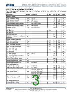
ELECTRICAL CHARACTERISTICS
VDD = VBST-VSW=12V, VSS=VSW = 0V, VEN=3.3V, No load at DRVH and DRVL, TA= +25°C, unless
otherwise noted.
Parameter
Symbol Condition
Min
Typ
Max
Units
Supply Current
VDD Shutdown Current
VDD quiescent current
VDD operating current
Floating driver quiescent current
Floating driver operating current
Leakage Current
ISHDN
IDDQ
IDDO
IBSTQ
IBSTO
ILK
VEN=0,
0
80
1
100
3.5
70
3
µA
µA
mA
µA
mA
μA
INL=INH=0
fsw=500kHz
INL=0, INH=0 or 1
fsw=500kHz
BST=SW=100V
2.8
55
2.1
0.05
1
Inputs
INL/INH High
2.4
V
V
V
INL/INH Low
1
INL/INH Hysteresis
0.6
INL/INH
resistance
internal
pull-down
RIN
185
kΩ
Under Voltage Protection
VDD rising threshold
VDDR
VDDF
4.6
4.1
4.6
4.1
5.0
4.5
5.0
4.5
5.4
4.9
5.4
4.9
0.7
V
V
VDD falling threshold
(BST-SW) rising threshold
(BST-SW) falling threshold
EN Input Logic Low
VBSTR
VBSTF
V
V
V
EN Input Logic High
1.5
V
EN Hysteresis
100
10
mV
µA
kΩ
EN Input Current
IEN
VEN=2V
EN internal pull-down resistance
Bootstrap Diode
REN
200
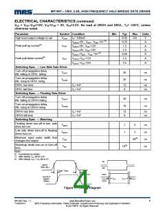
Bootstrap diode VF @ 100uA
Bootstrap diode VF @ 100mA
Bootstrap diode dynamic R
Low Side Gate Driver
Low level output voltage
High level output voltage to rail
VF1
VF2
RD
0.55
1
V
V
Ω
@ 100mA
2.7
VOLL
VOHL
IO=100mA
0.15
0.45
0.15
0.22
0.6
V
V
A
IO=-100mA
VDRVL=0V, VDD=4.5V (7)
Peak pull-up current(6)
IOHL
VDRVL=0V, VDD=12V
1.5
A
V
DRVL=0V, VDD=16V
2.5
0.25
2.5
A
A
A
A
VDRVL=VDD=4.5V (7)
VDRVL=VDD=12V
VDRVL=VDD=16V
Peak pull-down current(6)
IOLL
3.5
Floating Gate Driver
Low level output voltage
VOLH
IO=100mA
0.15
0.22
V
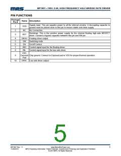
MP1907 Rev. 1.1
11/20/2013
www.MonolithicPower.com
MPS Proprietary Information. Patent Protected. Unauthorized Photocopy and Duplication Prohibited.
© 2013 MPS. All Rights Reserved.
3

 MPS [ MONOLITHIC POWER SYSTEMS ]