MP1498 – SYNCHRONOUS, STEP-DOWN CONVERTER WITH INTERNAL MOSFETS
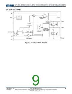
OPERATION
The MP1498 is a high-frequency, synchronous,
rectified, step-down, switch-mode converter
with built-in power MOSFETs. It offers a very
compact solution to achieve a continuous 2A
output current with excellent load and line
regulation over a wide input supply range.
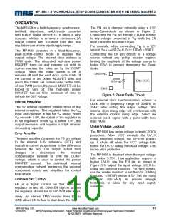
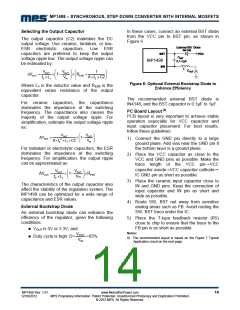
The EN pin is clamped internally using a 6.5V
series-Zener-diode as shown in Figure 2.
Connecting the EN pin through a pullup resistor
to any voltage connected to VIN limits the EN
input current to less than 100µA.
For example, when connecting VIN to a 12V
source, RPULLUP≥[(12V–6.5V) ÷ 100µA = 55kꢀ].
The MP1498 operates in a fixed-frequency,
peak-current–control mode to regulate the
output voltage. The internal clock initiates a
PWM cycle. The integrated high-side power
MOSFET turns on and remains on until its
current reaches the value set by the COMP
voltage. When the power switch is off, it
remains off until the next clock cycle starts. If
the current in the power MOSFET does not
reach the COMP set current value within 89%
of one PWM period, the power MOSFET will be
forced to turn off. The high-side power
MOSFET has an 80ns minimum off time to
refresh the BST voltage.
Connecting the EN pin directly to a voltage
source without any pullup resistor requires
limiting the amplitude of the voltage source to
below 6.5V to prevent damaging the Zener
diode.
EN/SYNC
Zener
EN LOGIC
6.5V-typ
GND
Figure 2: Zener Diode Circuit
For external clock synchronization, connect a
clock with a frequency range of 300kHz to
3MHz after setting the output voltage: The
internal clock rising edge will synchronize with
the external clock’s rising edge. Select an
external clock signal with a pulse-width less
than 700ns.
Internal Regulator
The 5V internal regulator powers most of the
internal circuitries. This regulator takes the VIN
input and operates in the full VIN range. When
VIN exceeds 5.0V, the output of the regulator is
in full regulation. When VIN is below 5.0V, the
output decreases and requires a 0.1µF ceramic
decoupling capacitor.
Under-Voltage Lockout
The MP1498 has under-voltage lockout (UVLO)
protection. When VCC exceeds the UVLO
rising threshold voltage, the MP1498 powers
up. It shuts off when the VCC voltage falls
below the UVLO falling threshold voltage. This
is non-latch protection.
Error Amplifier
The error amplifier compares the FB pin voltage
to the internal 0.8V reference (REF) and
outputs a current proportional to the difference
between the two. This output current then
charges
or
discharges
the
internal
The MP1498 is disabled when the input voltage
falls below 3.25V. If an application requires a
higher UVLO, use the EN pin as shown in
Figure 3 to adjust the input voltage UVLO by
using two external resistors. For best results,
use the enable resistors to set the UVLO falling
threshold (VSTOP) above 4.5V. Set the rising
threshold (VSTART) to provide enough
hysteresis to allow for any input supply
variations.
compensation network to form the COMP
voltage, which is used to control the power
MOSFET current. The optimized internal
compensation network minimizes the external
component counts and simplifies the control
loop design.
Enable/SYNC Control
EN is a digital control pin that turns the
regulator on and off. Drive EN high to turn on
the regulator, drive it low to turn it off after a 5μs
delay. An internal 1Mꢀ resistor from EN to
GND allows EN to float to shut down the chip.
MP1498 Rev. 1.01
12/18/2012
www.MonolithicPower.com
MPS Proprietary Information. Patent Protected. Unauthorized Photocopy and Duplication Prohibited.
© 2012 MPS. All Rights Reserved.
10

 MPS [ MONOLITHIC POWER SYSTEMS ]