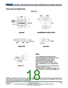
MP1498 – SYNCHRONOUS, STEP-DOWN CONVERTER WITH INTERNAL MOSFETS
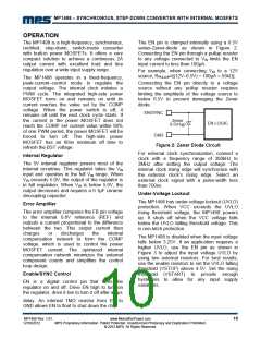
Selecting the Output Capacitor
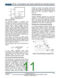
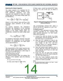
In these cases, connect an external BST diode
from the VCC pin to BST pin, as shown in
Figure 6
The output capacitor (C2) maintains the DC
output voltage. Use ceramic, tantalum, or low-
ESR electrolytic capacitors. Low ESR
capacitors are preferred to keep the output
voltage ripple low. The output voltage ripple can
be estimated by:
MP1498
VOUT
VOUT
1
VOUT
1
R
ESR
fS L1
V
8 fS C2
IN
Figure 6: Optional External Bootstrap Diode to
Enhance Efficiency
Where L1 is the inductor value and RESR is the
equivalent series resistance of the output
capacitor.
The recommended external BST diode is
For ceramic capacitors, the capacitance
dominates the impedance at the switching
frequency. The capacitance also causes the
majority of the output voltage ripple. For
simplification, estimate the output voltage ripple
as:
IN4148, and the BST capacitor is 0.1µF to 1μF.
PC Board Layout (8)
PCB layout is very important to achieve stable
operation especially for VCC capacitor and
input capacitor placement. For best results,
follow these guidelines:
VOUT
8 fS2 L1 C2
VOUT
ΔVOUT
1
1) Connect the GND pin directly to a large
ground plane. Add vias near the GND pin if
the bottom layer is a ground plane.
V
IN
For tantalum or electrolytic capacitors, the ESR
dominates the impedance at the switching
frequency. For simplification, the output ripple
can be approximated as:
2) Place the VCC capacitor as close to the
VCC and GND pins as possible. Make the
trace length of the VCC pin→VCC
capacitor anode՜VCC capacitor cathode→
IC GND pin as short as possible.
VOUT
VOUT
ΔVOUT
1
RESR
fS L1
V
IN
3) Place the ceramic input capacitor close to
IN and GND pins. Keep the connection of
input capacitor and IN pin as short and
wide as possible.
The characteristics of the output capacitor also
affect the stability of the regulation system. The
MP1498 can be optimized for a wide range of
capacitance and ESR values.
4) Route SW, BST net away from sensitive
analog areas such as FB. Avoid routing the
SW, BST trace under the IC.
External Bootstrap Diode
An external bootstrap diode can enhance the
efficiency of the regulator, given the following
conditions:
5) Place the T-type feedback resistor (R5)
close to chip to ensure that the trace to the
FB pin is as short as possible.
Notes:
VOUT is 5V or 3.3V; and
VOUT
Duty cycle is high: D=
>65%
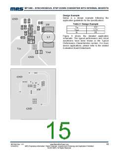
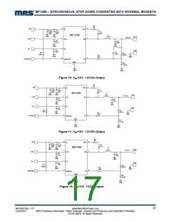
8) The recommended layout is based on the Figure 7 Typical
Application circuit on the next page.
VIN
MP1498 Rev. 1.01
12/18/2012
www.MonolithicPower.com
MPS Proprietary Information. Patent Protected. Unauthorized Photocopy and Duplication Prohibited.
© 2012 MPS. All Rights Reserved.
14

 MPS [ MONOLITHIC POWER SYSTEMS ]