Freescale Semiconductor, Inc.
Electrical Specifications
Tables of Data
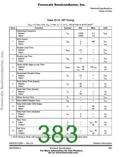
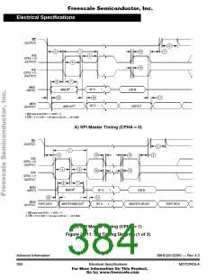
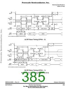
Table 20-15. SPI Timing
(VDD = 5.0 Vdc ±10%, VSS = 0 Vdc, TA = TL to TH , 200 pF load on all SPI pins)(1)
Num
Function
Operating Frequency
Symbol
Min
Max
Unit
f
f
Master
Slave
1/256
1/256
1/2
1/2
op
eclk
SCK Period
Master
Slave
t
t
t
1
2
3
4
5
2
2
256
—
cyc
sck
cyc
Enable Lead Time
Master
Slave
t
t
t
1/2
1
—
—
sck
lead
cyc
Enable Lag Time
Master
Slave
t
t
t
1/2
1
—
—
sck
lag
cyc
Clock (SCK) High or Low Time
Master
Slave
t
t
− 30
− 30
t
128 t
ns
ns
cyc
wsck
cyc
—
cyc
Sequential Transfer Delay
Master
Slave
t
t
t
1/2
1
—
—
sck
td
cyc
Data Setup Time (Inputs)
Master
Slave
t
6
7
30
30
—
—
ns
ns
su
Data Hold Time (Inputs)
Master
Slave
t
0
30
—
—
ns
ns
hi
t
t
8
9
Slave Access Time
—
—
1
1
a
cyc
cyc
t
t
Slave MISO Disable Time
dis
Data Valid (after SCK Edge)
Master
Slave
t
10
11
—
—
50
50
ns
ns
v
Data Hold Time (Outputs)
Master
Slave
t
0
0
—
—
ns
ns
ho
Rise Time
Input
Output
t
t
t
− 30
30
12
13
—
—
ns
ns
ri
cyc
t
ro
Fall Time
Input
Output
t
− 30
30
—
—
ns
ns
fi
cyc
t
fo
1. All AC timing is shown with respect to 20% VDD and 70% VDD levels unless otherwise noted.
68HC(9)12D60 — Rev 4.0
Advance Information
383
MOTOROLA
Electrical Specifications
For More Information On This Product,
Go to: www.freescale.com

 MOTOROLA [ MOTOROLA ]