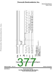
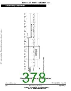
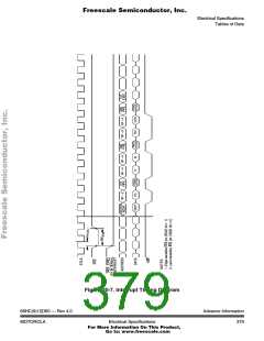
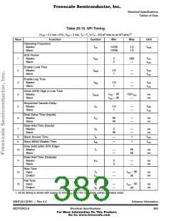
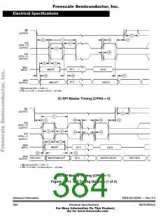
Freescale Semiconductor, Inc.
Electrical Specifications
Tables of Data
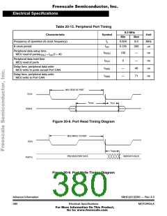
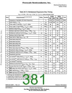
Table 20-14. Multiplexed Expansion Bus Timing
VDD = 5.0 Vdc ± 10%, VSS = 0 Vdc, TA = TL to TH, unless otherwise noted
8 MHz
2MHz
Unit
(1), (2), (3), (4)
Num
Delay Symbol
Characteristic
Min Max Min Max
f
Frequency of operation (E-clock frequency)
0.004 8.0 0.004 2.0 MHz
0.125 250 0.5 250
o
Cycle timet = 1/f
t
cyc
1
2
—
−4
−2
27
—
−18
—
—
—
—
—
—
—
18
—
—
18
µs
ns
ns
ns
ns
ns
ns
ns
ns
ns
ns
ns
ns
ns
ns
ns
ns
cyc
o
Pulse width, E lowPW = t /2 + delay
PW
58
60
246
248
EL
cyc
EL
EH
(5)
PW
3
Pulse width, E high PW = t /2 + delay
EH
cyc
Address delay timet = t /4 + delay
t
AD
5
58
152
AD
cyc
Address valid time to ECLK riset = PW − t
t
AV
7
0
94
107
20
AV
EL
AD
Multiplexed address hold timet
Address Hold to Data Valid
= t /4 + delay
t
MAH
8
13
20
MAH
cyc
t
9
AHDS
Data Hold to High Zt
= t − 20
t
10
38
47
132
165
DHZ
AD
DHZ
t
11 Read data setup time
12 Read data hold time
13 Write data delay time
14 Write data hold time
25
0
25
0
DSR
t
DHR
t
DDW
DHW
t
20
13
20
83
(5)
t
t
15
16
17
Write data setup time
Read/write delay timet
t
= PW − t
DSW EH DDW
DSW
= t /4 + delay
49
49
143
143
RWD
cyc
RWD
Read/write valid time to E riset
= PW − t
t
t
9
103
20
RWV
EL
RWD
RWV
18 Read/write hold time
20
RWH
(6)
t
19
20
21
22
23
24
25
Low strobe delay timet
= t /4 + delay
cyc
LSD
LSD
(6)
t
—
—
—
—
8
9
103
20
ns
ns
ns
ns
Low strobe valid time to E riset
= PW − t
EL LSD
LSV
LSV
(6)
t
20
Low strobe hold time
LSH
(5)
t
t
t
42
35
39
323
223
133
Address access time
t
= t − t − t
ACCA
ACCE
DBED
ACCA cyc AD DSR
(5)
Access time from E rise
t
= PW − t
EH DSR
ACCE
(5)
ns
ns
ns
DBE delay from ECLK rise
t
= t /4 + delay
DBED
cyc
DBE valid timet
= PW − t
t
—
21
–3
115
–3
DBE
EH
DBED
DBE
t
26 DBE hold time from ECLK fall
10
10
DBEH
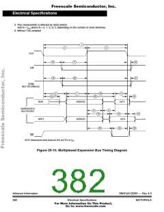
1. All timings are calculated for normal port drives.
2. Crystal input is required to be within 45% to 55% duty.
3. Reduced drive must be off to meet these timings.
4. Unequalled loading of pins will affect relative timing numbers.
68HC(9)12D60 — Rev 4.0
Advance Information
381
MOTOROLA
Electrical Specifications
For More Information On This Product,
Go to: www.freescale.com

 MOTOROLA [ MOTOROLA ]