Freescale Semiconductor, Inc.
Electrical Specifications
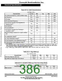
Table 20-16. CGM Characteristics
5.0 Volts 10%
Characteristic
PLL reference frequency, crystal oscillator range
Bus frequency
Symbol
Min.
0.5
Typ.
Max.
8
Unit
MHz
MHz
MHz
MHz
f
REF
f
0.004
2.5
8
BUS
f
VCO range
8
VCO
f
VCO Limp-Home frequency
Lock Detector transition from Acquisition to
0.5
1
2.5
VCOMIN
∆
3%
4%
—
trk
(1)
Tracking mode
∆
Lock Detection
0%
1.5%
2.5%
—
—
Lock
∆
Un-Lock Detection
0.5%
unl
Lock Detector transition from Tracking to
∆
6%
1
8%
—
unt
(1)
Acquisition mode
Minimum leakage resistance on crystal oscillator
pins
r
MΩ
leak
(2)
PLL Stabilization delay
(3)
t
3
1
2
ms
ms
ms
PLL Total Stabilization Delay
stab
(3)
t
PLLON Acquisition mode stabilization delay.
acq
(3)
t
PLLON tracking mode stabilization delay.
al
1. AUTO bit set
2. PLL stabilization delay is highly dependent on operational requirement and external component values (i.e. crystal, XFC
filter component values|). Note (3) shows typical delay values for a typical configuration. Appropriate XFC filter values
should be chosen based on operational requirement of system.
3. f
= 4MHz, f
= 8MHz (REFDV = #$00, SYNR = #$01), XFC:Cs = 33nF, Cp = 3.3nF, Rs = 2.7KΩ.
REF
BUS
Table 20-17. Key Wake-up
VDD = 5.0V dc 10%
Characteristic
Symbol
Min.
2
Max.
Unit
µs
t
STOP Key Wake-Up Filter time
10
KWSTP
t
Key Wake-Up Single Pulse Time Interval
20
µs
KWSP
Table 20-18. msCAN12 Wake-up Time from Sleep Mode
VDD = 5.0V dc 10%, VSS = 0 Vdc, TA = TL to TH, unless otherwise noted
Characteristic
Symbol
Min.
Max.
Unit
t
Wake-Up time
2
5
µs
wup
Advance Information
386
68HC(9)12D60 — Rev 4.0
MOTOROLA
Electrical Specifications
For More Information On This Product,
Go to: www.freescale.com

 MOTOROLA [ MOTOROLA ]