Freescale Semiconductor, Inc.
Pulse Width Modulator
PWM Register Description
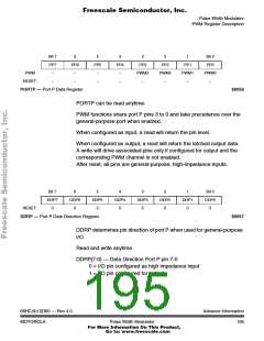
Bit 7
PP7
–
6
PP6
–
5
PP5
–
4
PP4
–
3
PP3
PWM3
–
2
PP2
PWM2
–
1
Bit 0
PP0
PP1
PWM
PWM1
–
PWM0
–
RESET:
–
–
–
–
PORTP — Port P Data Register
$0056
PORTP can be read anytime.
PWM functions share port P pins 3 to 0 and take precedence over the
general-purpose port when enabled.
When configured as input, a read will return the pin level.
When configured as output, a read will return the latched output data.
A write will drive associated pins only if configured for output and the
corresponding PWM channel is not enabled.
After reset, all pins are general-purpose, high-impedance inputs.
Bit 7
DDP7
0
6
DDP6
0
5
DDP5
0
4
DDP4
0
3
DDP3
0
2
DDP2
0
1
DDP1
0
Bit 0
DDP0
0
RESET:
DDRP — Port P Data Direction Register
$0057
DDRP determines pin direction of port P when used for general-purpose
I/O.
Read and write anytime.
DDRP[7:0] — Data Direction Port P pin 7-0
0 = I/O pin configured as high impedance input
1 = I/O pin configured for output.
68HC(9)12D60 — Rev 4.0
MOTOROLA
Advance Information
Pulse Width Modulator
195
For More Information On This Product,
Go to: www.freescale.com

 MOTOROLA [ MOTOROLA ]