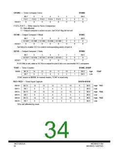
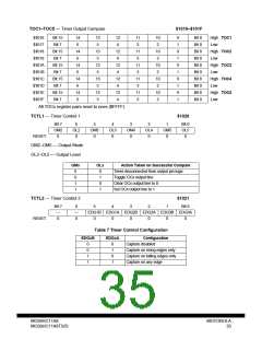
TOC1–TOC5 — Timer Output Compare
$1016–$101F
$1016
$1017
$1018
$1019
$101A
$101B
$101C
$101D
$101E
$101F
Bit 15
Bit 7
14
6
13
5
12
4
11
3
10
2
9
1
9
1
9
1
9
1
9
1
Bit 8
Bit 0
Bit 8
Bit 0
Bit 8
Bit 0
Bit 8
Bit 0
Bit 8
Bit 0
High TOC1
Low
Bit 15
Bit 7
14
6
13
5
12
4
11
3
10
2
High TOC2
Low
Bit 15
Bit 7
14
6
13
5
12
4
11
3
10
2
High TOC3
Low
Bit 15
Bit 7
14
6
13
5
12
4
11
3
10
2
High TOC4
Low
Bit 15
Bit 7
14
6
13
5
12
4
11
3
10
2
High TOC5
Low
All TOCx register pairs reset to ones ($FFFF).
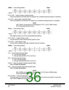
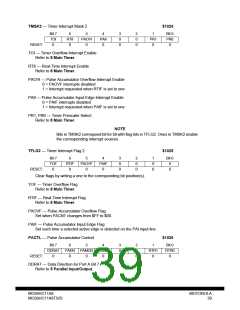
TCTL1 — Timer Control 1
$1020
Bit 7
OM2
0
6
OL2
0
5
OM3
0
4
OL3
0
3
OM4
0
2
OL4
0
1
OM5
0
Bit 0
OL5
0
RESET:
OM2–OM5 — Output Mode
OL2–OL5 — Output Level
OMx
OLx
Action Taken on Successful Compare
0
0
1
1
0
1
0
1
Timer disconnected from output pin logic
Toggle OCx output line
Clear OCx output line to 0
Set OCx output line to 1
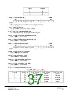
TCTL2 — Timer Control 2
$1021
Bit 7
—
6
—
0
5
4
3
2
1
Bit 0
EDG1B EDG1A EDG2B EDG2A EDG3B EDG3A
RESET:
0
0
0
0
0
0
0
Table 7 Timer Control Configuration
EDGxB
EDGxA
Configuration
Capture disabled
0
0
1
1
0
1
0
1
Capture on rising edges only
Capture on falling edges only
Capture on any edge
MC68HC11A8
MC68HC11A8TS/D
MOTOROLA
35

 MOTOROLA [ MOTOROLA ]