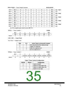
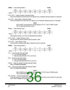
TMSK1 — Timer Interrupt Mask 1
$1022
Bit 7
OC1I
0
6
OC2I
0
5
OC3I
0
4
OC4I
0
3
OC5I
0
2
IC1I
0
1
IC2I
0
Bit 0
IC3I
0
RESET:
OC1I–OC5I — Output Compare x Interrupt Enable
If the OCxI enable bit is set when the OCxF flag bit is set, a hardware interrupt sequence is requested.
IC1I–IC3I — Input Capture x Interrupt Enable
If the ICxI enable bit is set when the ICxF flag bit is set, a hardware interrupt sequence is requested.
NOTE
Bits in TMSK1 correspond bit for bit with flag bits in TFLG1. Ones in TMSK1 enable
the corresponding interrupt sources.
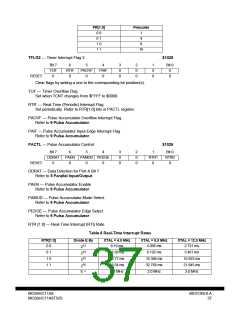
TFLG1 — Timer Interrupt Flag 1
$1023
Bit 7
OC1F
0
6
OC2F
0
5
OC3F
0
4
OC4F
0
3
OC5F
0
2
IC1F
0
1
IC2F
0
Bit 0
IC3F
0
RESET:
Clear flags by writing a one to the corresponding bit position(s).
OC1F–OC5F — Output Compare x Flag
Set each time the counter matches output compare x value.
IC1F–IC3F — Input Capture x Flag
Set each time a selected active edge is detected on the ICx input line.
TMSK2 — Timer Interrupt Mask 2
$1024
Bit 7
TOI
0
6
RTII
0
5
PAOVI
0
4
PAII
0
3
0
0
2
0
0
1
PR1
0
Bit 0
PR0
0
RESET:
TOI — Timer Overflow Interrupt Enable
0 = TOF interrupts disabled
1 = Interrupt requested when TOF is set to one
RTII — Real-Time Interrupt Enable
0 = RTIF interrupts disabled
1 = Interrupt requested when RTIF is set to one
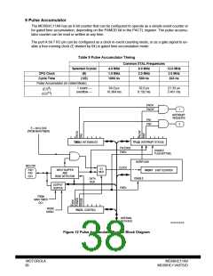
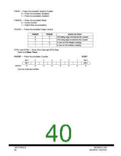
PAOVI — Pulse Accumulator Overflow Interrupt Enable
Refer to 9 Pulse Accumulator.
PAII — Pulse Accumulator Input Edge Interrupt Enable
Refer to 9 Pulse Accumulator.
NOTE
Bits in TMSK2 correspond bit for bit with flag bits in TFLG2. Ones in TMSK2 enable
the corresponding interrupt sources.
PR1 and PR0 — Timer Prescaler Select
In normal modes, PR1 and PR0 can only be written once, and the write must be within 64 cycles after
reset. Refer to Table 6 for specific timing values.
MOTOROLA
36
MC68HC11A8
MC68HC11A8TS/D

 MOTOROLA [ MOTOROLA ]