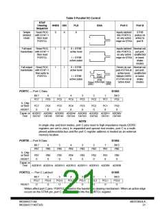
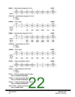
DDRC — Data Direction Register for Port C
$1007
Bit 7
DDC7
0
6
DDC6
0
5
DDC5
0
4
DDC4
0
3
DDC3
0
2
DDC2
0
1
DDC1
0
Bit 0
DDC0
0
RESET:
DDC[7:0] — Data Direction Register for Port C
0 = Input
1 = Output
PORTD — Port D Data
$1008
Bit 7
6
0
0
5
PD5
0
4
PD4
0
3
PD3
0
2
PD2
0
1
PD1
0
Bit 0
PD0
0
0
0
RESET:
Alt. Pin
Func.:
—
—
SS
SCK
MOSI
MISO
TxD
RxD
DDRD — Data Direction Register for Port D
$1009
Bit 7
0
6
0
5
DDD5
0
4
DDD4
0
3
DDD3
0
2
DDD2
0
1
DDD1
0
Bit 0
DDD0
0
RESET:
0
0
Alt. Pin
Func.:
—
—
PD5/
SS
PD4/
SCK
PD3/
MOSI
PD2/
MISO
PD1/
TxD
PD0/
RxD
DDD[5:0] — Data Direction for Port D
0 = Input
1 = Output
PORTE — Port E Data
$100A
Bit 7
PE7
U
6
PE6
U
5
PE5
U
4
PE4
U
3
PE3
U
2
PE2
U
1
PE1
U
Bit 0
PE0
U
RESET:
Alt. Pin
Func.:
AN7
AN6
AN5
AN4
AN3
AN2
AN1
AN0
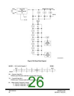
PACTL — Pulse Accumulator Control
$1026
Bit 7
DDRA7
0
6
PAEN
0
5
4
3
0
0
2
0
0
1
RTR1
0
Bit 0
RTR0
0
PAMOD PEDGE
RESET:
0
0
DDRA7 — Data Direction for Port A Bit 7
0 = Input
1 = Output
PAEN — Pulse Accumulator System Enable
Refer to 9 Pulse Accumulator.
PAMOD — Pulse Accumulator Mode
Refer to 9 Pulse Accumulator.
PEDGE — Pulse Accumulator Edge Control
Refer to 9 Pulse Accumulator.
RTR1, RTR0 — Real-Time Interrupt Rate
Refer to 8 Main Timer.
MOTOROLA
22
MC68HC11A8
MC68HC11A8TS/D

 MOTOROLA [ MOTOROLA ]