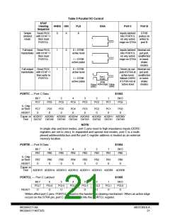
Table 5 Parallel I/O Control
STAF
Clearing
Sequence
HNDS OIN
PLS
EGA
Port C
Port B
Simple
strobed
mode
Read PIOC
with STAF=1
then read
0
X
X
Inputs latched
into PORTCL pulses on
on any active
edge on STRA
STRB
0
1
writes to
port B
PORTCL
Full input
handshake with STAF=1
then read
Read PIOC
1
0
0 = STRB
active level
Inputs latched Normal out-
into PORTCL put port,
on any active unaffected
edge on STRA in hand-
shake
1
0
PORTCL
1 = STRB
active pulse
modes
Full output Read PIOC
handshake with STAF=1
then write to
1
1
0 = STRB
active level
Driven as out- Normal out-
puts if STRA at
active level,
follows DDRC
if STRA not at
active level
put port,
unaffected
in hand-
shake
0
Port C
Driven
PORTCL
1 = STRB
active pulse
1
STRA
Active Edge
Follow
DDRC
modes
Follow
DDRC
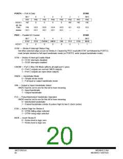
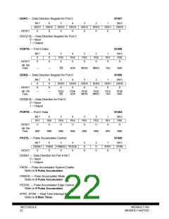
PORTC — Port C Data
$1003
Bit 7
PC7
6
5
4
3
2
1
Bit 0
PC0
PC6
PC5
PC4
PC3
PC2
PC1
S. Chip
or Boot:
PC7
0
PC6
0
PC5
0
PC4
0
PC3
0
PC2
0
PC1
0
PC0
0
RESET:
Expan.or ADDR7/ ADDR6/ ADDR5/ ADDR4/ ADDR3/ ADDR2/ ADDR1/ ADDR0/
Test:
DATA7 DATA6 DATA5 DATA4 DATA3 DATA2 DATA1 DATA0
NOTE
In single chip and boot modes, port C pins reset to high impedance inputs (DDRC
registers are set to zero). In expanded and special test modes, port C is a multi-
plexed address/data bus and the port C register address is treated as an external
memory location.
PORTB — Port B Data
$1004
Bit 7
6
5
4
3
2
1
Bit 0
PB0
PB7
PB6
PB5
PB4
PB3
PB2
PB1
S. Chip
or Boot:
PB7
0
PB6
0
PB5
0
PB4
0
PB3
0
PB2
0
PB1
0
PB0
0
RESET:
Expan.or
Test:
ADDR15 ADDR14 ADDR13 ADDR12 ADDR11 ADDR10 ADDR9 ADDR8
PORTCL — Port C Latched
$1005
Bit 7
PCL7
U
6
PCL6
U
5
PCL5
U
4
PCL4
U
3
PCL3
U
2
PCL2
U
1
PCL1
U
Bit 0
PCL0
U
RESET:
Writes affect port C pins. PORTCL is used in the handshake clearing mechanism. When an active edge
occurs on the STRA pin, port C data is latched into the PORTCL register.
MC68HC11A8
MC68HC11A8TS/D
MOTOROLA
21

 MOTOROLA [ MOTOROLA ]